Method for improving defects of LCOS process
A process defect and process technology, applied in the field of improving LCOS process defects, can solve problems affecting reflection effects, etc., achieve the effect of reducing the number of defects and preventing the diffusion of copper ions
- Summary
- Abstract
- Description
- Claims
- Application Information
AI Technical Summary
Problems solved by technology
Method used
Image
Examples
Embodiment 1
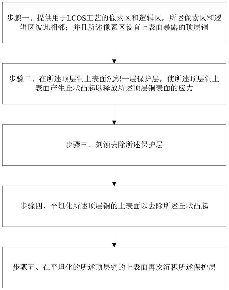
[0033] The invention provides a method for improving LCOS process defects, such as image 3 as shown, image 3 Shown as the method for improving LCOS process defects of the present invention, the method at least includes the following steps:
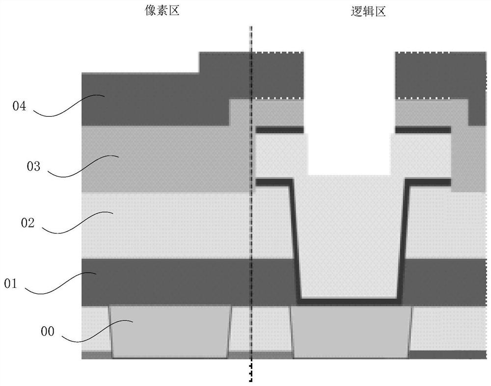
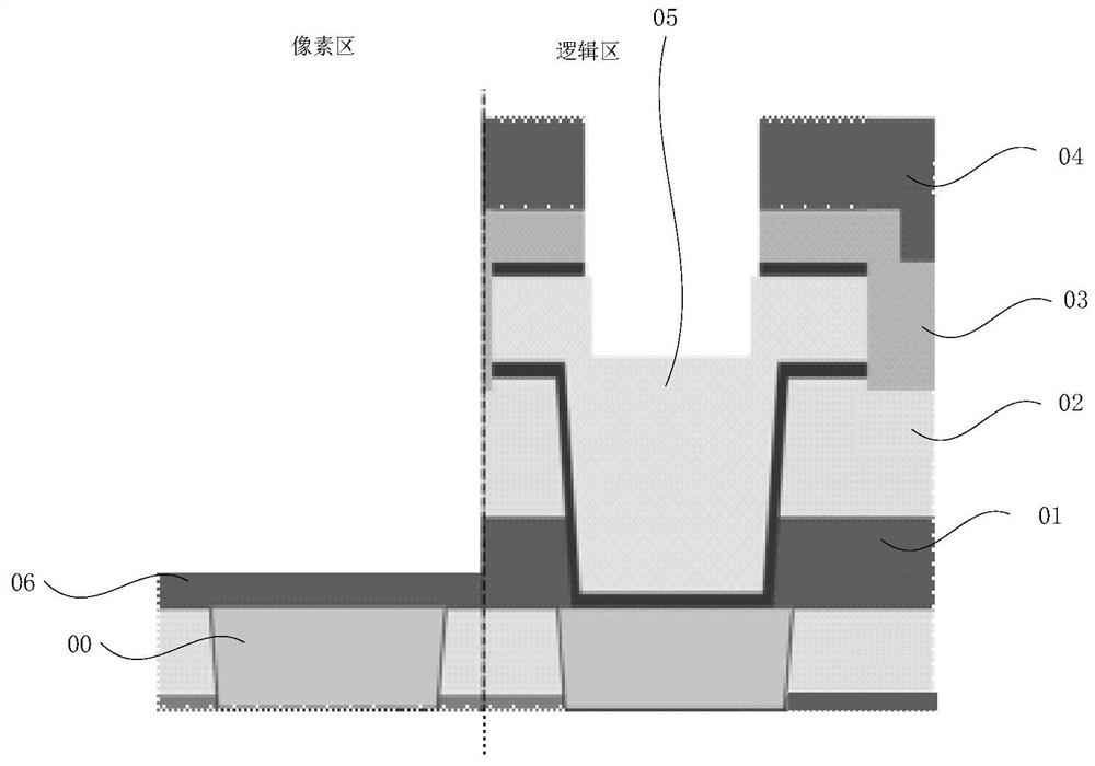
[0034] Step 1, providing a pixel region and a logic region for the LCOS process, the pixel region and the logic region are adjacent to each other; and the pixel region is provided with a top layer copper exposed on the upper surface; as figure 2 as shown, figure 2 It is shown as a structural schematic diagram of the pixel area and logic area in the present invention; figure 2 In the LCOS (micro-display on silicon) process, the pixel area and the logic area are separated from each other by a vertical dotted line, and the pixel area (pixel) and the logic area (logic) are adjacent to each other; and the pixel area (pixel) ) has a top layer of copper 00 exposed on the upper surface;
[0035] Further in the present invention, the thick...
Embodiment 2
[0047] The present invention provides a method for improving LCOS process defects. The difference between this embodiment and Embodiment 1 is that the protective layer in step 2 of this embodiment is an NDC (nitrogen-doped silicon carbide film) layer, and at the same time The protective layer in step five of this embodiment is an NDC (nitrogen-doped silicon carbide film) layer.
Embodiment 3
[0049] The present invention provides a method for improving LCOS process defects. The protective layer in step 2 of this embodiment is a silicon nitride layer or an NDC (nitrogen-doped silicon carbide film) layer. At the same time, the protective layer in step five of this embodiment is a silicon nitride layer or an NDC (nitrogen-doped silicon carbide film) layer.
[0050] To sum up, the present invention releases the stress on the copper surface and then deposits a protective layer to prevent the diffusion of copper ions without adding a mask. After the process is optimized, the number of defects on the copper surface is significantly reduced. Therefore, the present invention effectively overcomes various shortcomings in the prior art and has high industrial application value.
PUM
 Abstract
Description
Claims
Application Information


