InAs/GaSb buffer layer, silicon-based antimonide semiconductor material, preparation method of silicon-based antimonide semiconductor material, and component
A silicon-based antimonide and buffer layer technology, which is applied in the structural details of semiconductor lasers and other directions, can solve the problems of limiting the performance improvement of laser devices, many defects in the active area, and poor material quality.
- Summary
- Abstract
- Description
- Claims
- Application Information
AI Technical Summary
Problems solved by technology
Method used
Image

Examples
Embodiment 1
[0046] This embodiment provides a method for preparing a GaSb / InAs buffer layer and a silicon-based antimonide semiconductor material, comprising the following steps:
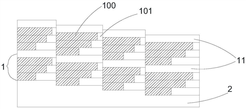
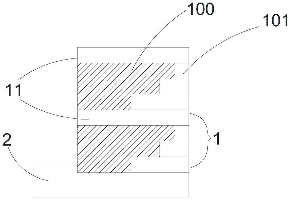
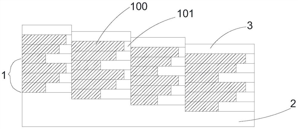
[0047] (1) On a silicon substrate with an inclination angle, the inclination angle is 2.86°, and the step length is about 6nm. GaSb and InAs layers are grown sequentially to control their distribution on the steps. The coverage ratio of the steps is 1:1.
[0048] The growth parameters include: the substrate temperature is 400°C, and the III / V beam current ratio is 1:1.
[0049] (1)GaSb growth, and control the coverage of GaSb on the step with the inclined substrate: first grow 1ML thick GaSb on the substrate, control the migration time of GaSb on the substrate step to 0.5s, and the migration speed to 0.5ML / s. First, the Ga source and the Sb source are turned on, and the coverage of GaSb is observed by RHEED (High Energy Electron Diffraction). After 0.5s, the Ga source and the Sb source are turned off, and th...
Embodiment 2
[0068] This embodiment provides a method for preparing a GaSb / InAs buffer layer and a silicon-based antimonide semiconductor material, comprising the following steps:
[0069] (1) On a silicon substrate with an inclination angle, the inclination angle is 2.86°, and the step length is about 6nm. GaSb and InAs layers are grown sequentially to control their distribution on the steps. The coverage ratio on the steps is 1:1.
[0070] The growth parameters include: the substrate temperature is 450°C, and the III / V beam current ratio is 1:5.
[0071] (1)GaSb growth, and control the coverage of GaSb on the step with the inclined substrate: first grow 1ML thick GaSb on the substrate, control the migration time of GaSb on the substrate step to 0.5s, and the migration speed to 0.5ML / s. First, the Ga source and the Sb source are turned on, and the coverage of GaSb is observed by RHEED (High Energy Electron Diffraction). After 0.5s, the Ga source and the Sb source are turned off, and th...
Embodiment 3
[0087] This embodiment provides a method for preparing a GaSb / InAs buffer layer and a silicon-based antimonide semiconductor material, comprising the following steps:
[0088] (1) On a silicon substrate with an inclination angle, the inclination angle is 2.86°, and the step length is about 6nm. GaSb and InAs layers are grown sequentially to control their distribution on the steps. The coverage ratio on the steps is 1:1.
[0089] The growth parameters include: the substrate temperature is 550°C, and the III / V beam current ratio is 1:10.
[0090] (1)GaSb growth, and control the coverage of GaSb on the step with the inclined substrate: first grow 1ML thick GaSb on the substrate, control the migration time of GaSb on the substrate step to 0.5s, and the migration speed to 0.5ML / s. First, the Ga source and the Sb source are turned on, and the coverage of GaSb is observed by RHEED (High Energy Electron Diffraction). After 0.5s, the Ga source and the Sb source are turned off, and t...
PUM
| Property | Measurement | Unit |
|---|---|---|
| thickness | aaaaa | aaaaa |
| thickness | aaaaa | aaaaa |
| lattice constant | aaaaa | aaaaa |
Abstract
Description
Claims
Application Information
 - R&D
- Intellectual Property
- Life Sciences
- Materials
- Tech Scout
- Unparalleled Data Quality
- Higher Quality Content
- 60% Fewer Hallucinations
Browse by: Latest US Patents, China's latest patents, Technical Efficacy Thesaurus, Application Domain, Technology Topic, Popular Technical Reports.
© 2025 PatSnap. All rights reserved.Legal|Privacy policy|Modern Slavery Act Transparency Statement|Sitemap|About US| Contact US: help@patsnap.com