Patterned substrate, preparation method thereof, light emitting diode and preparation method of light emitting diode

A patterned substrate and substrate technology, applied in the direction of electrical components, circuits, semiconductor devices, etc., can solve the problems of decreased epitaxy surface ratio, epitaxy difficulties, unfavorable epitaxial epitaxial layers, etc., to improve quality and increase light output effect, the effect of reducing the dislocation density

Inactive Publication Date: 2021-04-23
FUJIAN JING AN OPTOELECTRONICS CO LTD
View PDF4 Cites 1 Cited by
  • Summary
  • Abstract
  • Description
  • Claims
  • Application Information

AI Technical Summary

Problems solved by technology

However, the proportion of the epitaxial surface of the current patterned substrate is limited; and when the area of ​​the epitaxial surface is too small, it is easy to cause difficulties in epitaxy, which is not conducive to the epitaxy of high-quality epitaxial layers

Method used


Image

  • Patterned substrate, preparation method thereof, light emitting diode and preparation method of light emitting diode
  • Patterned substrate, preparation method thereof, light emitting diode and preparation method of light emitting diode
  • Patterned substrate, preparation method thereof, light emitting diode and preparation method of light emitting diode

Examples


Embodiment 1

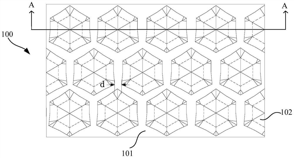
[0092] This embodiment provides a patterned substrate, which includes a substrate and a number of periodic and closely arranged pattern structures formed on the surface of the substrate, and the minimum distance d between adjacent pattern structures is less than or Equal to 0.1 μm. The graphic structure includes a first part formed on the surface of the substrate and a second part formed above the first part. The first part includes: a cylindrical part formed with an inscribed circle inscribed with the upper surface of the first part as a bottom surface. and a plurality of first protrusions and a plurality of second protrusions uniformly arranged around the cylindrical portion; the first protrusions and the second protrusions are spaced apart from each other, and the cross-sectional area of ​​the first protrusions is greater than or equal to the second The cross-sectional area of ​​the protrusion. Since the proportion of the epitaxial surface of the substrate exposed between ...

Embodiment 2

[0101] This embodiment discloses a method for preparing a patterned substrate, including: providing a substrate, forming several pattern structures on the surface of the substrate, and the pattern structures are periodically arranged closely on the surface of the substrate; adjacent patterns The minimum distance between structures is less than or equal to 0.1 μm. Wherein, the graphic structure includes a first part located on the surface of the substrate and a second part located above the first part, and the first part includes: a cylindrical part formed with an inscribed circle inscribed with the upper surface of the first part as a bottom surface; And the first protrusion and the second protrusion evenly arranged around the cylindrical part; area.

[0102] In one embodiment of the present invention, refer to Figures 5a-5f and 2a-2b, including:

[0103] S101: Provide a substrate, and form a nucleation inhibiting material layer on the surface of the substrate, where the m...

Embodiment 3

[0119] This embodiment discloses a light emitting diode, refer to Image 6 ; The light-emitting diode includes a substrate and an epitaxial layer formed on the surface of the substrate, wherein the substrate is a patterned substrate as in Embodiment 1 or 2, and the epitaxial layer is formed on the side of the patterned substrate with a pattern structure.

[0120] Specifically, refer to Image 6 , on the patterned side of the patterned substrate 100, the epitaxial layer composed of the first semiconductor layer 110, the active layer 120 and the second semiconductor layer 130 opposite to the type of the first semiconductor layer 110 is included in sequence; The first electrode 140 is formed on the second semiconductor layer 130 , and the second electrode 150 is formed on the first semiconductor layer 110 . Optionally, a transparent conductive layer, such as ITO, is further formed on the first semiconductor layer 130 and the second semiconductor layer 140; both the first electro...


PUM

PropertyMeasurementUnit
thicknessaaaaaaaaaa
heightaaaaaaaaaa

Abstract

The invention discloses a patterned substrate, a preparation method thereof, a light emitting diode and a preparation method of the light emitting diode. In one embodiment, the patterned substrate comprises a substrate and a plurality of patterned structures which are formed on the surface of the substrate and are periodically and tightly arranged, and the minimum distance between the adjacent patterned structures is smaller than or equal to 0.1 [mu]m; the pattern structure comprises a first part formed on the surface of the substrate and a second part formed above the first part, and the first part comprises a cylindrical part, and a first protruding part and a second protruding part which are uniformly distributed around the cylindrical part; and the first protruding parts and the second protruding parts are arranged at intervals, and the cross section area of the first protruding parts is larger than or equal to that of the second protruding parts. Therefore, the patterned substrate and the light emitting diode provided by the invention can effectively reduce the area and dislocation density of the epitaxial crystal surface and improve the light emitting efficiency; and the scattering efficiency of the light can be further improved, and the brightness of the LED is improved.

Description

technical field [0001] The invention relates to the technical field of semiconductor devices, in particular to a patterned substrate, a light emitting diode and a preparation method. Background technique [0002] Due to the lattice mismatch and thermal expansion coefficient mismatch between the heterogeneous substrate and the epitaxial material, the interior of the heterogeneous epitaxial material has a high dislocation density, which will cause carrier leakage and reduce the internal quantum efficiency. [0003] In order to suppress the generation and slip of dislocations and obtain an epitaxial layer with low dislocation density and high crystal quality, a patterned substrate technology has been developed in the prior art. The patterned substrate technology makes a pattern with a fine structure on the surface of the heterogeneous substrate, and then performs LED material epitaxy on the surface of the patterned substrate. The patterned interface changes the growth process ...

Claims


Application Information

Patent Timeline
Patent Type & Authority Applications(China)
IPC IPC(8): H01L33/22H01L33/10H01L33/00
CPCH01L33/007H01L33/10H01L33/22
Inventor 苏贤达李彬彬霍曜李瑞评吴福仁梅晓阳
Owner FUJIAN JING AN OPTOELECTRONICS CO LTD
Why Eureka
Try Eureka