Check patentability & draft patents in minutes with Patsnap Eureka AI!

Resistive random access memory and preparation method thereof

A resistive memory, resistive variable technology, applied in semiconductor devices, electric solid state devices, electrical components, etc., can solve the problems of restricting the industrial application of resistive memory, uncontrollability, etc., to improve discreteness, improve consistency, The effect of broad application prospects

Active Publication Date: 2021-04-23
SHANGHAI INTEGRATED CIRCUIT EQUIP & MATERIALS IND INNOVATION CENT CO +1
View PDF12 Cites 2 Cited by
  • Summary
  • Abstract
  • Description
  • Claims
  • Application Information

AI Technical Summary

Problems solved by technology

It can be seen that since the overlapping area of ​​the upper and lower electrodes is too large (almost equal from the figure), the oxygen vacancy conductive channel formed in the oxide resistive layer is usually very uncontrollable, which further leads to the resistance of the resistive memory. The electrical characteristics of the cells are also highly discrete, which seriously restricts the industrial application of resistive memory.

Method used


Image

  • Resistive random access memory and preparation method thereof
  • Resistive random access memory and preparation method thereof
  • Resistive random access memory and preparation method thereof

Examples


Embodiment Construction

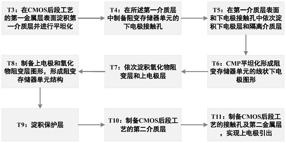
[0040] Attached below Figure 2-11 , the specific embodiment of the present invention will be further described in detail.

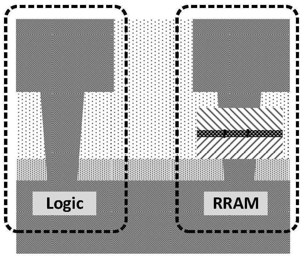
[0041] see first Figure 11 , Figure 11 Shown is a schematic cross-sectional view of a resistive memory product formed by the resistive memory manufacturing method proposed in the present invention. As shown in the figure, the resistive memory includes at least one resistive memory unit; it is characterized in that the resistive memory unit includes:

[0042] The first dielectric layer has a lower electrode contact hole inside, the lower electrode contact hole includes a linear lower electrode and an isolation dielectric layer, one side of the linear lower electrode is close to the side wall of the lower electrode contact hole, so The other side of the linear lower electrode is close to the isolation dielectric layer;

[0043] On the upper surface of the first dielectric layer, the oxide resistive pattern and the upper electrode are sequentially sta...


PUM


Abstract

The invention discloses a resistive random access memory and a preparation method thereof. The method comprises the following steps of: depositing a first dielectric layer on the surface of a first metal layer of a CMOS back-end process; preparing a lower electrode contact hole in the first dielectric layer; sequentially depositing a lower electrode layer and an isolation dielectric layer in the first dielectric layer and the lower electrode contact hole to prepare a linear lower electrode of a resistive random access memory unit; sequentially depositing an oxide resistive random access layer and an upper electrode layer, and preparing an upper electrode and an oxide resistive random access pattern to form a resistive random access memory unit; depositing protective layers on the surfaces and the side surfaces of the upper electrode and the oxide resistance change pattern and the surface of the first dielectric layer, and preparing a second dielectric layer of the CMOS back-end process; and preparing a contact hole and a second metal layer of the CMOS back-end process on the second dielectric layer so as to lead out the upper electrode of the resistive random access memory unit, and leading out the lower electrode of the resistive random access memory unit through the first metal layer. Therefore, the formation region of an oxygen vacancy conductive channel in the resistive random access layer is limited, so that the device consistency is improved.

Description

technical field [0001] The invention belongs to the field of integrated circuit manufacturing, and in particular relates to a resistive variable memory and a preparation method thereof. Background technique [0002] Resistive Random Access Memory (RRAM) is a new type of non-volatile memory, which has high speed, low power consumption, non-volatility, high integration and complementary metal oxide semiconductor (Complementary Metal Oxide Semiconductor) Semiconductor, CMOS) process compatibility and other advantages have become one of the research hotspots in the field of new memory in recent years, and even commercial products have appeared. [0003] The resistive memory cell is the core of the resistive memory technology. The resistive memory cell based on transition metal oxide has been extensively studied due to its high compatibility with the mainstream CMOS process. It usually adopts a structure similar to a parallel plate capacitor, that is, it contains A sandwich stru...

Claims


Application Information

Patent Timeline
Patent Type & Authority Applications(China)
IPC IPC(8): H01L45/00H01L27/24
CPCH10B63/00H10N70/821H10N70/24H10N70/011
Inventor 郭奥
Owner SHANGHAI INTEGRATED CIRCUIT EQUIP & MATERIALS IND INNOVATION CENT CO
Features
  • R&D
  • Intellectual Property
  • Life Sciences
  • Materials
  • Tech Scout
  • Unparalleled Data Quality
  • Higher Quality Content
  • 60% Fewer Hallucinations
Learn More