Polarization beam splitter structure and polarization beam splitting method

A polarization beam splitter and coupling waveguide technology, which is applied in the direction of instruments, light guides, optics, etc., can solve the problems of high manufacturing requirements of nano-groove structures, deterioration of photonic integrated device performance, and impossible elimination of birefringence phenomenon, etc., and meet the technical requirements Not harsh, simple structure, low insertion loss effect

Active Publication Date: 2021-04-27
QXP TECH INC
View PDF8 Cites 4 Cited by
  • Summary
  • Abstract
  • Description
  • Claims
  • Application Information

AI Technical Summary

Problems solved by technology

A serious problem usually exists in devices with small waveguide dimensions: the birefringence cannot be eliminated, which leads to a large phase difference between different modes, which seriously deteriorates the performance of photonic integrated devices
Among them, the manufacturing process of the nano-groove structure requires high requirements; the manufacturing tolerance of the bridge waveguide structure to the waveguide width and waveguide spacing is relatively small, and the insertion loss is relatively large; although the tapered waveguide structure can achieve high extinction ratio and large process tolerance Polarization Beam splitters, but the device is not compact enough and requires special design

Method used


Image

  • Polarization beam splitter structure and polarization beam splitting method
  • Polarization beam splitter structure and polarization beam splitting method
  • Polarization beam splitter structure and polarization beam splitting method

Examples


Embodiment 1

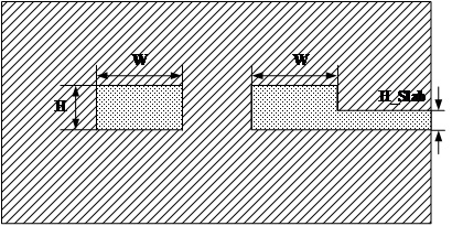
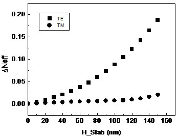
[0036] The material of the designed waveguide structure is silicon with a refractive index of 3.455, and the buffer layer and upper cover layer are silicon dioxide with a refractive index of 1.445. The height H of the bar-shaped straight waveguide structure is 220nm, and the width W is 450nm, and the height H of the ridge-shaped straight waveguide structure is 220nm, and the width is 450nm. The difference in refractive index (△Neff) between the TE mode and the TM mode of the ridge straight waveguide and the strip straight waveguide calculated by the finite element analysis method varies with the height of the slab region (H_Slab) as follows image 3 As shown, the strip straight waveguide structure corresponds to the case of H_Slab=0. It can be seen that with the increase of H_Slab, the refractive index of the TE mode increases gradually, and the difference between the refractive index of the TE mode and the strip straight waveguide becomes larger, while the change of the refra...


PUM


Abstract

The invention discloses a polarization beam splitter structure and a polarization beam splitting method, of which the input area of the polarization beam splitter structure comprises a first input waveguide structure of a strip-shaped straight waveguide structure and a second input waveguide structure of a ridge-shaped straight waveguide structure. A coupling area comprises a first coupling waveguide structure of a strip-shaped straight waveguide structure and a second coupling waveguide structure of a ridge-shaped straight waveguide structure, wherein an input port of the first coupling waveguide structure is connected with an output port of the first input waveguide structure, and an input port of the second coupling waveguide structure is connected with an output port of the second input waveguide structure. An output area comprises a first output waveguide structure of a strip-shaped straight waveguide structure and a second output waveguide structure of a ridge-shaped straight waveguide structure, wherein an input port of the first output waveguide structure is connected with an output port of the first coupling waveguide structure, and an input port of the second output waveguide structure is connected with an output port of the second coupling waveguide structure. The beam splitter is compact in structure, and can realize the characteristics of large process tolerance, low insertion loss, high extinction ratio, wide transmission bandwidth and the like.

Description

technical field [0001] The invention belongs to the field of photon integration, and in particular relates to a polarization beam splitter structure and a polarization beam splitting method. Background technique [0002] The rapid development of photonic integration mainly depends on the successful development and application of a large number of functional devices with low insertion loss and compact structure. A serious problem usually exists in devices with small waveguide dimensions: the birefringence phenomenon cannot be eliminated, which leads to large phase differences between different modes, which seriously deteriorates the performance of photonic integrated devices. In addition, in the field of optical communication long-distance transmission, polarization multiplexing technology has been successfully applied to expand the transmission capacity of communication systems. To enable individual control of the polarization states, the transverse electric mode (TE) and t...

Claims


Application Information

Patent Timeline
IPC IPC(8): G02B6/10G02B6/126
CPCG02B6/105G02B6/126
Inventor 郭菲布兰特·埃弗雷特·李特尔程东
Owner QXP TECH INC
Why Eureka
Try Eureka