Check patentability & draft patents in minutes with Patsnap Eureka AI!

Shield gate trench MOSFET device with electrostatic protection capability and manufacturing method thereof

A technology of electrostatic protection and shielding grid, which is applied in semiconductor/solid-state device manufacturing, electric solid-state devices, electrical components, etc., can solve problems affecting device performance, adverse effects of devices, poor shielding effect, etc. Complexity, the effect of reducing steps

Pending Publication Date: 2021-04-27
无锡惠芯半导体有限公司
View PDF1 Cites 2 Cited by
  • Summary
  • Abstract
  • Description
  • Claims
  • Application Information

AI Technical Summary

Problems solved by technology

If the etching strength is increased during etching back, the interlayer oxide layer h1 of the shielding gate may be too small, and the interlayer oxide layer plays the role of isolating the control gate electrode and the shielding gate electrode. If the thickness is insufficient or voids appear, the Adverse effects on device IGSS (gate-to-source short circuit current)
[0005] 2. If in order to solve the above-mentioned problem that may cause the interlayer oxide layer h1 of the shield gate to be too small, you can consider increasing the thickness of the interlayer oxide layer, so that there will be two results A. The trench depth h2 remains unchanged, and the gate polysilicon h3 B. The gate polysilicon h3 remains unchanged, and the trench depth h2 increases, which will affect the device BV (drain-source breakdown voltage) / IDSS (saturated drain-source current) performance
like Figure 4 As shown, such residues are easy to fall off in the subsequent process, resulting in gate-source short circuit and affecting yield

Method used


Image

  • Shield gate trench MOSFET device with electrostatic protection capability and manufacturing method thereof
  • Shield gate trench MOSFET device with electrostatic protection capability and manufacturing method thereof
  • Shield gate trench MOSFET device with electrostatic protection capability and manufacturing method thereof

Examples


Embodiment Construction

[0045] The specific implementation manner of the present invention will be described below in conjunction with the accompanying drawings.

[0046] The invention discloses a shielding gate trench MOSFET device with electrostatic protection capability and a manufacturing method thereof. Figure 5 ~ Figure 12 The steps of one embodiment of the fabrication method are shown. specific:

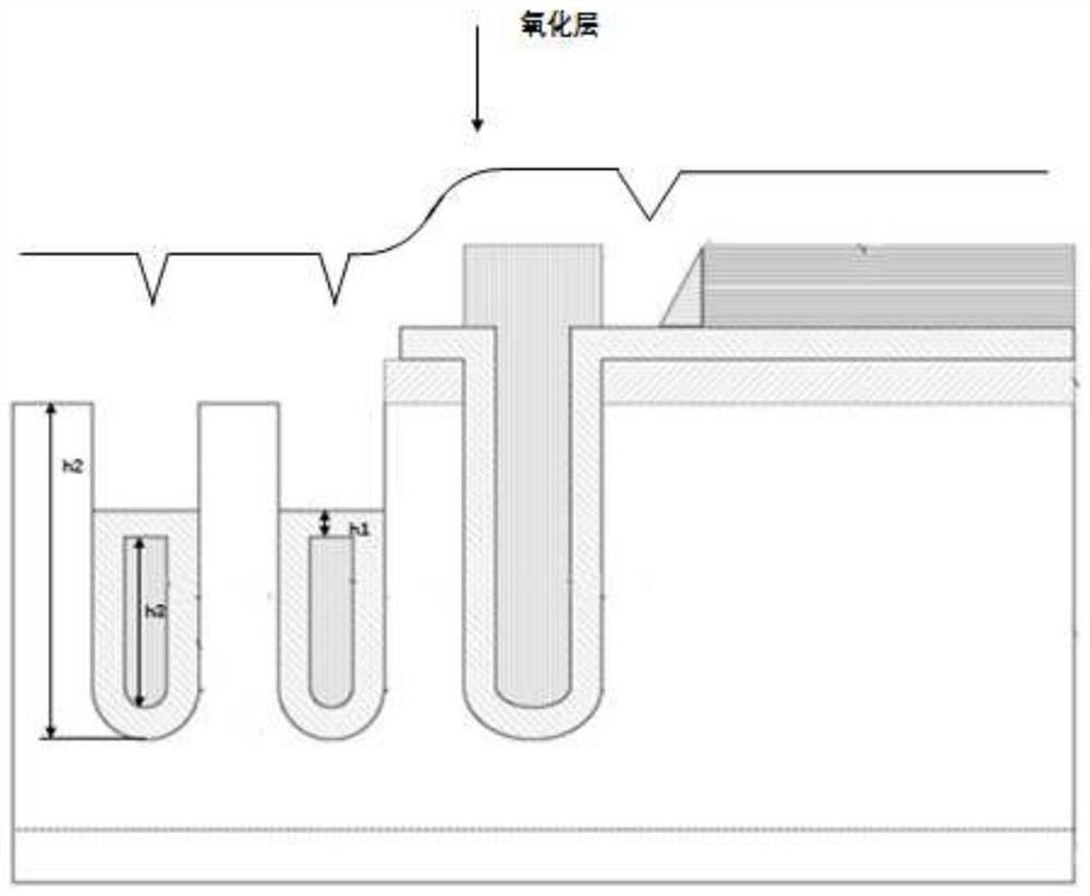
[0047] Figure 5 is a schematic diagram of step S1. Such as Figure 5 As shown, in step S1 , an N-type substrate 1 is provided, and an N-type epitaxial layer 2 is formed on the substrate 1 . The N-type epitaxial layer 2 is located on the N-type substrate 1 . A patterned mask layer is formed on the epitaxial layer 2 , and the upper surface of the epitaxial layer 2 is etched by a dry etching process to obtain the first trench 3 and the second trench 4 .

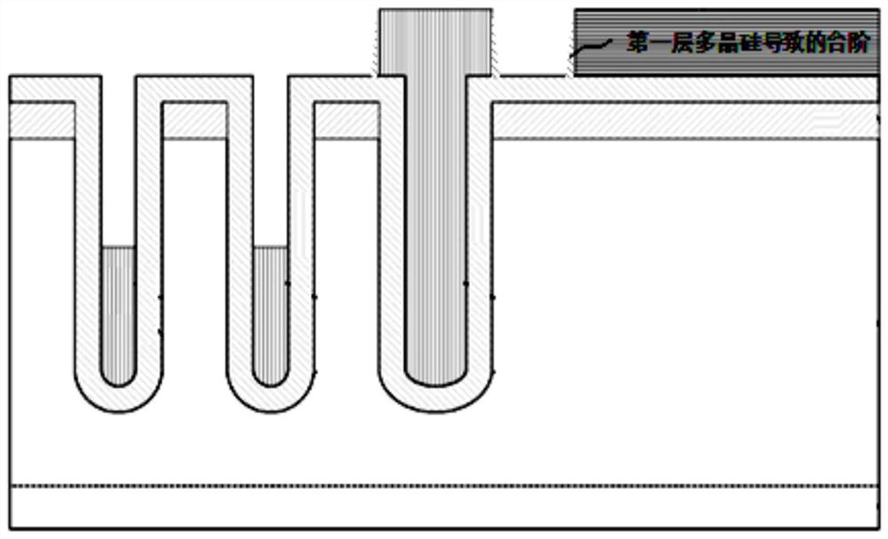
[0048] Step S2 is a step of depositing a first polysilicon layer to form a shielding gate. See step S2 Image 6 , Figure 7 shown.

[0049...


PUM


Abstract

The invention relates to a shielding gate trench MOSFET device with electrostatic protection capability and a manufacturing method. The method comprises steps of providing a substrate, and forming an epitaxial layer on the upper surface of the substrate; etching the epitaxial layer to obtain a first groove and a second groove; forming a first dielectric layer and a first polycrystalline silicon layer in the first groove and the second groove; forming a shielding gate in the second trench; depositing a second polycrystalline silicon layer, wherein the second polycrystalline silicon layer comprises a second polycrystalline silicon layer block II filled in the upper region of the second trench and a second polycrystalline silicon layer block IV positioned on the side edge of the first trench; forming a body region beside the second trench; forming a source region on the surface layer of the body region, and synchronously forming a plurality of ESD protection diodes with NPN structures on the second polycrystalline silicon layer block IV; according to the method, the influence of steps formed by primary polycrystalline silicon deposition on morphology and device reliability in the prior art is avoided, and the method has great progress for the prior art.

Description

technical field [0001] The invention relates to a MOSFET device and a manufacturing method thereof, in particular to a shielding gate trench MOSFET device with electrostatic protection capability and a manufacturing method thereof. Background technique [0002] There is a thin gate oxide layer between the gate and source of MOSFET, which is vulnerable to external unexpected high voltage impact during device packaging, transportation, assembly and use, and generates a high electric field on the gate, making the gate The insulation breakdown of the dielectric under high electric field causes the device to fail. Therefore, in some practical applications, it is necessary to provide electrostatic discharge (ESD) protection for the gate of the MOSFET. A common practice is to connect a diode protection unit in parallel between the gate and source of the MOSFET. When the voltage generated by electrostatic discharge (ESD) is higher than the breakdown voltage of the diode (the breakd...

Claims


Application Information

Patent Timeline
Patent Type & Authority Applications(China)
IPC IPC(8): H01L29/78H01L29/06H01L21/336H01L29/423H01L27/02
CPCH01L27/0251H01L29/0603H01L29/0684H01L29/4236H01L29/66477H01L29/78
Inventor 徐彩云
Owner 无锡惠芯半导体有限公司
Features
  • R&D
  • Intellectual Property
  • Life Sciences
  • Materials
  • Tech Scout
  • Unparalleled Data Quality
  • Higher Quality Content
  • 60% Fewer Hallucinations
Learn More