Laser etching equipment for chip silicon wafer and chip production process

A laser etching, silicon wafer technology, applied in laser welding equipment, welding equipment, metal processing equipment, etc., can solve the problems of long adjustment time for template replacement, inconvenient adjustment of laser etching focus, etc.

Active Publication Date: 2021-05-07
深圳市凤翔光电电子有限公司
View PDF5 Cites 3 Cited by
  • Summary
  • Abstract
  • Description
  • Claims
  • Application Information

AI Technical Summary

Problems solved by technology

[0006] Aiming at the deficiencies of the prior art, the present invention provides a chip silicon wafer laser etching equipment, which is convenient for adjusting the focus position of laser etching and the adjustment of etching area. The advantages of precise size and position control solve the problems of inconvenient laser etching focus adjustment and long adjustment time for template replacement

Method used


Image

  • Laser etching equipment for chip silicon wafer and chip production process
  • Laser etching equipment for chip silicon wafer and chip production process
  • Laser etching equipment for chip silicon wafer and chip production process

Examples


Embodiment Construction

[0034] The following will clearly and completely describe the technical solutions in the embodiments of the present invention with reference to the accompanying drawings in the embodiments of the present invention. Obviously, the described embodiments are only some, not all, embodiments of the present invention. Based on the embodiments of the present invention, all other embodiments obtained by persons of ordinary skill in the art without making creative efforts belong to the protection scope of the present invention.

[0035] As introduced in the background technology, there are deficiencies in the prior art. In order to solve the above technical problems, the present application proposes a chip silicon wafer laser etching equipment.

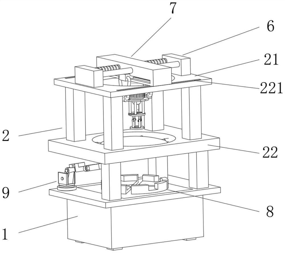
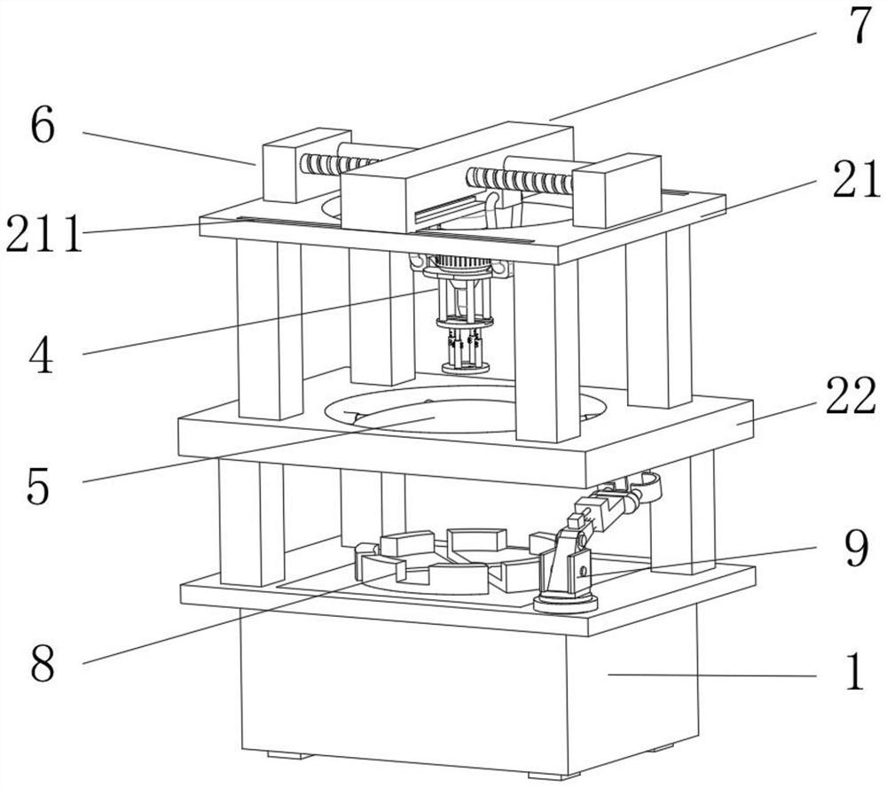
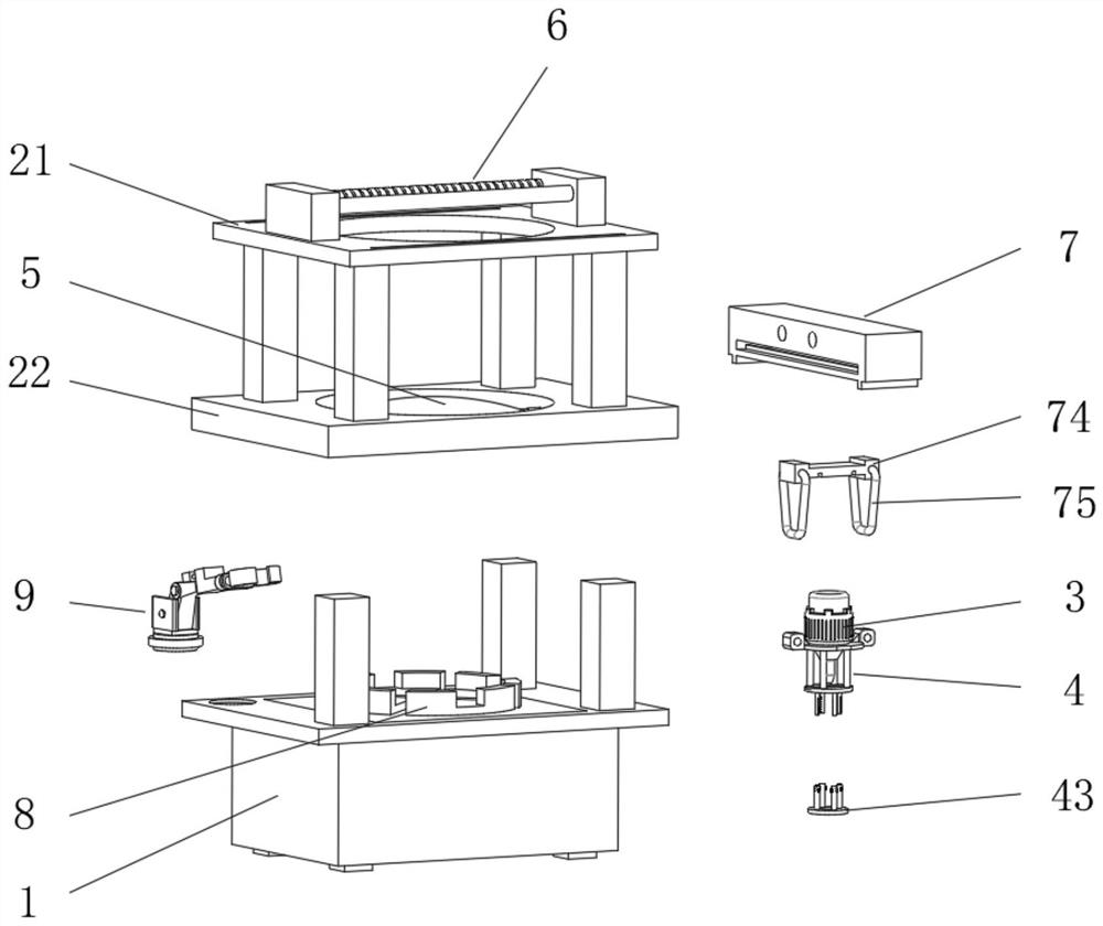
[0036] see Figure 1-9 , a chip silicon wafer laser etching equipment, including a workbench 1, a double-layer mounting frame 2, a laser gun 3 and a mechanical arm 9, the bottom of the laser gun 3 is provided with an adjustable hoisting frame 4,...


PUM


Abstract

The invention relates to the technical field of laser etching and discloses laser etching equipment for a chip silicon wafer and a chip production process. The equipment comprises a worktable, a double-layer mounting rack, a laser gun and a mechanical arm, wherein an adjustable hoisting rack is arranged at the bottom end of the laser gun and comprises a top hoisting rack, an etching template mounting rack and a movable lens rack. By arranging a primary lens capable of being disassembled and replaced, a laser beam emitted by the laser gun is subjected to a filtering action of the etching template and is collected preliminarily under the action of the primary lens, so that the laser beam can be controlled to generate a focal point on the surface of a wafer and the size of a spot etched by the laser beam every time is determined. Moreover, the vertical position of the etched focal point can be changed conveniently by replacing the primary lens, so that the size of the spot can be adjusted conveniently to determine the depth and size of a circuit groove formed by etching every time.

Description

technical field [0001] The invention relates to the technical field of laser etching, in particular to a chip silicon wafer laser etching equipment and a chip production process. Background technique [0002] Wafer refers to the silicon wafer used to make silicon semiconductor circuits, and its raw material is silicon. High-purity polycrystalline silicon is dissolved and mixed with silicon crystal seeds, and then slowly pulled out to form cylindrical single crystal silicon. After the silicon ingot is ground, polished, and sliced, it forms a silicon wafer, that is, a wafer. At present, domestic wafer production lines are mainly 8-inch and 12-inch. The main processing methods of wafers are sheet processing and batch processing, that is, one or more wafers are processed at the same time. As semiconductor feature sizes become smaller and processing and measurement equipment become more advanced, laser etching of silicon wafers during silicon wafer processing is an important s...

Claims


Application Information

Patent Timeline
Patent Type & Authority Applications(China)
IPC IPC(8): B23K26/362B23K26/70H01L21/67H01L21/687H01L21/302B23K101/40
CPCB23K26/362B23K26/702H01L21/67011H01L21/68757H01L21/302B23K2101/40
Inventor 李俊
Owner 深圳市凤翔光电电子有限公司
Why Eureka
Try Eureka