Corrosion process for reducing thickness deviation value of damaged layer of wafer

A wafer and damage layer technology, applied in the field of semiconductor silicon wafer processing, can solve the problems of uneven corrosion thickness and large deviation value, etc.

Inactive Publication Date: 2021-05-07
TIANJIN ZHONGHUAN ADVANCED MATERIAL TECH +1
View PDF12 Cites 0 Cited by
  • Summary
  • Abstract
  • Description
  • Claims
  • Application Information

AI Technical Summary

Problems solved by technology

[0003] The invention provides an etching process for reducing the deviation value of the damaged layer thickness of the wafer, which solves the technical problems of uneven corrosion thickness and large deviation value in the prior art

Method used


Image

  • Corrosion process for reducing thickness deviation value of damaged layer of wafer
  • Corrosion process for reducing thickness deviation value of damaged layer of wafer

Examples


Embodiment 1

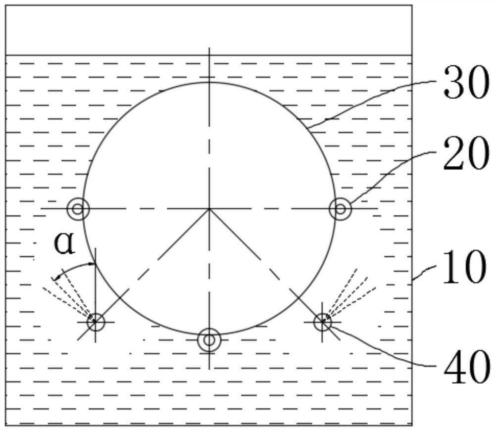
[0041] The wafer 30 diameter is the wafer of 300mm to etch, specifically as follows:

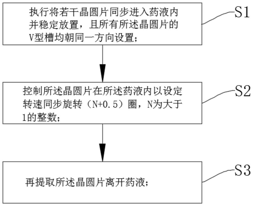
[0042] S1: Put the wafer 30 into the liquid medicine and place it stably

[0043] A plurality of wafers 30 are vertically clamped by a mobile manipulator and vertically enter the liquid medicine, wherein the V-shaped grooves of all wafers 30 are vertically set upwards; the time taken from entering the liquid medicine to placing and leaving for 8s.

[0044] Wherein, the mass concentration of the medicinal solution is a pure solution of potassium hydroxide of 45%, the constant temperature of the medicinal solution is 82° C., and the circulating flow rate of the medicinal solution is 30 L / min; Nitrogen gas is bubbled upward, and the angle α between the direction of nitrogen gas injection and the vertical diameter of the wafer 30 is 45°.

[0045] S2: controlling the wafer 30 to rotate synchronously

[0046] After the wafer 30 is placed stably, control the adjustment lever 20 to rotate the wafer...


PUM


Abstract

The invention provides a corrosion process for reducing the thickness deviation value of a damaged layer of a wafer. The process comprises the steps that: a plurality of wafers are made to synchronously enter a solution and are stably placed, and the V-shaped grooves of all the wafers face the same direction; the wafers are controlled to synchronously rotate (N+ 0.5) circles in the solution at a set rotating speed, wherein N is an integer greater than 1; and the wafers are extracted to leave the solution. The duration from a time point when the wafers enter the solution to a time point when the wafers are stably placed is the same as the duration from a time point when the still standing of the wafers is completed to a time point when the wafers are completely taken out of the solution. According to the corrosion process of the invention, the parts of the wafers, which firstly enter the solution in a groove body, firstly leave the solution, so that the difference value of the corrosion thicknesses of two sides of each wafer is reduced to the greatest extent, the uniformity and consistency of the corrosion thickness of the wafers are improved, a foundation is laid for obtaining qualified geometric parameters for subsequent polishing processing, and the production efficiency is improved.

Description

technical field [0001] The invention belongs to the technical field of semiconductor silicon wafer processing, and in particular relates to an etching process for reducing the thickness deviation value of the damaged layer of the wafer. Background technique [0002] After the semiconductor silicon wafer is thinned and ground, there is a layer of mechanical damage on the surface of the silicon wafer, mainly silicon, which must be removed before polishing. At present, alkaline solution is used to remove it. The uniformity of the thickness of the corrosion damage layer directly affects The TTV and physical and chemical test results in the geometric parameters even affect the production of the subsequent process. In the existing etching process, the wafer enters the etching tank and then is taken out according to the original state of placement, but this operation is easy to make the part that enters first be taken out later, instead of the first-in-first-out setting, resulting ...

Claims


Application Information

Patent Timeline
Patent Type & Authority Applications(China)
IPC IPC(8): H01L21/306H01L21/67
CPCH01L21/30604H01L21/67253
Inventor 刘姣龙刘建伟刘园武卫由佰玲裴坤羽孙晨光王彦君祝斌常雪岩杨春雪谢艳袁祥龙张宏杰刘秒吕莹徐荣清
Owner TIANJIN ZHONGHUAN ADVANCED MATERIAL TECH
Why Eureka
Try Eureka