Substrate treatment apparatus

A substrate processing device and substrate technology, which is applied in the direction of lasers, laser welding equipment, electrical components, etc., can solve the problems of limited etching uniformity, difficulty in meeting the miniaturization of circuit patterns, etc., and achieve excellent etching process and high-performance etching Process, the effect of increasing the amount of etching

Pending Publication Date: 2021-05-07
SEMES CO LTD
View PDF0 Cites 0 Cited by
  • Summary
  • Abstract
  • Description
  • Claims
  • Application Information

AI Technical Summary

Problems solved by technology

However, due to the limited etching uniformity and etching amount of conventional etching methods, it may be difficult to meet the miniaturization of circuit patterns.

Method used


Image

  • Substrate treatment apparatus
  • Substrate treatment apparatus
  • Substrate treatment apparatus

Examples


Embodiment Construction

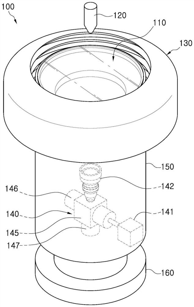
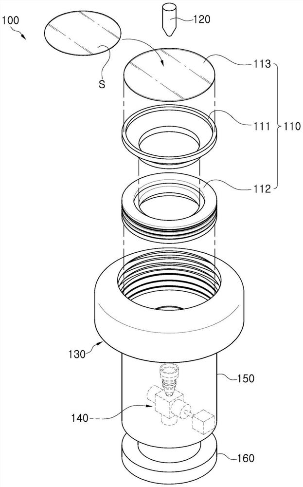
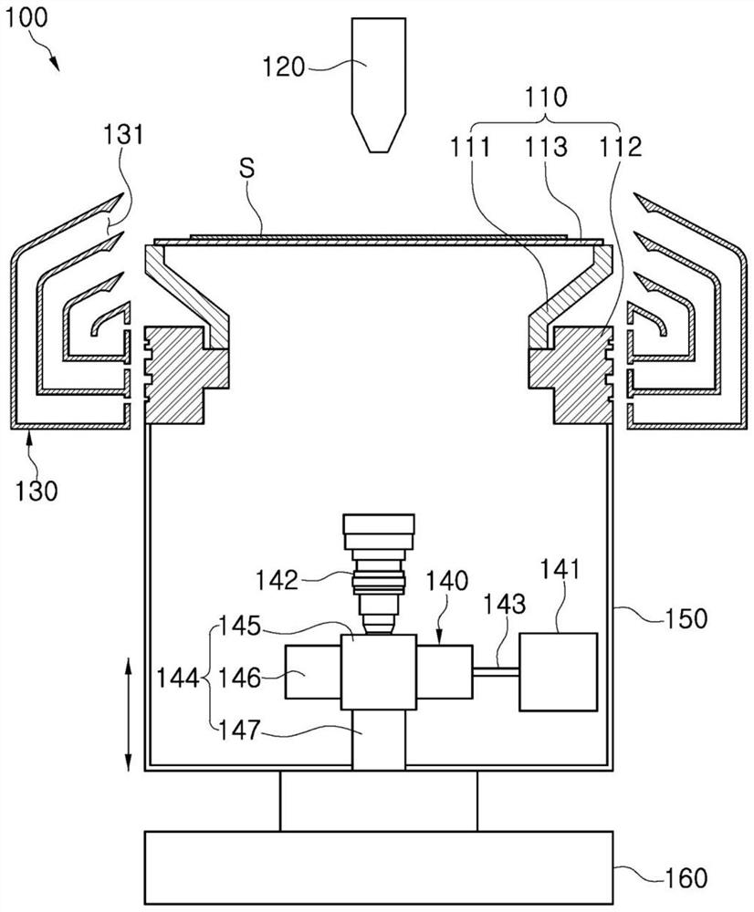
[0048] Hereinafter, embodiments of the present invention will be described in detail with reference to the accompanying drawings so that those having ordinary knowledge in the technical field to which the present invention pertains can easily implement. The present invention can be realized in various forms and is not limited to the embodiments described here.

[0049] In order to clearly describe the present invention, parts irrelevant to the description are omitted, and the same reference numerals are attached to the same or similar constituent elements throughout the entire specification.

[0050] In addition, in each embodiment, the same reference numerals are used for the constituent elements having the same structure, and only the representative embodiment will be described, and in the remaining other embodiments, only the structures different from the representative embodiment will be described. illustrate.

[0051]Throughout the specification, when it is said that a c...


PUM


Abstract

Disclosed is a substrate treatment apparatus including a rotation unit that supports and rotates a substrate, a chemical discharge unit that discharges a chemical solution to the rotation unit, a chemical recovery unit disposed close to the rotation unit and configured to recover the chemical solution scattering from the rotation unit, and a laser irradiation unit that applies a laser beam to the substrate and heats the substrate. Thus, the temperature of the substrate is adjusted by irradiating the substrate with the laser, and the amount of etching by the chemical solution can be increased.

Description

technical field [0001] The present invention relates to a substrate processing apparatus, and more specifically, to a substrate processing apparatus that can be used for manufacturing semiconductors. Background technique [0002] As semiconductor elements become denser, more integrated, and more functional, the need for miniaturization of circuit patterns is further increasing. For example, 3D V-NAND flash memory (3D V-NAND flash memory), which is used as a storage element among various semiconductor devices, has been manufactured with 24-layer and 32-layer stacked circuits, and recently with 64-layer stacked circuits. [0003] Circuits stacked in multiple layers should be properly evaporated and etched to be fabricated as designed. Therefore, in order to manufacture 3D V-NAND flash memory with more than 64 layers, excellent etching technology and evaporation technology may be required. [0004] On the other hand, among various processes for manufacturing semiconductor ele...

Claims


Application Information

Patent Timeline
Patent Type & Authority Applications(China)
IPC IPC(8): H01L21/67
CPCH01L21/6708H01L21/67115H01L21/67248H01L21/6719H01L21/67063H01L21/68764B23K26/362H01S3/0007H01L21/6715H01L21/68742H01L21/6704C09K13/04H01L21/30604
Inventor 郑暎大金源根李智暎郑智训金泰信吴世勋许弼覠朴炫九
Owner SEMES CO LTD
Why Eureka
Try Eureka