Two-stage excitation self-destruction chip based on array type pore channels, and preparation method thereof

An array and channel technology, which is applied in the field of information security and semiconductor devices, can solve the problems of complex structure design, poor safety and reliability, etc., and achieve the effects of ensuring safety, reducing dose and chip area, and realizing directional and fixed-point damage

Active Publication Date: 2021-05-11
SICHUAN UNIV
View PDF8 Cites 1 Cited by
  • Summary
  • Abstract
  • Description
  • Claims
  • Application Information

AI Technical Summary

Problems solved by technology

The patent application number 200480013540.8 discloses a device structure that utilizes reactant chemical reagents to corrode storage media, but the design of the structure is complex and its safety and reliability are not good enough

Method used


Image

  • Two-stage excitation self-destruction chip based on array type pore channels, and preparation method thereof
  • Two-stage excitation self-destruction chip based on array type pore channels, and preparation method thereof
  • Two-stage excitation self-destruction chip based on array type pore channels, and preparation method thereof

Examples


Embodiment 1

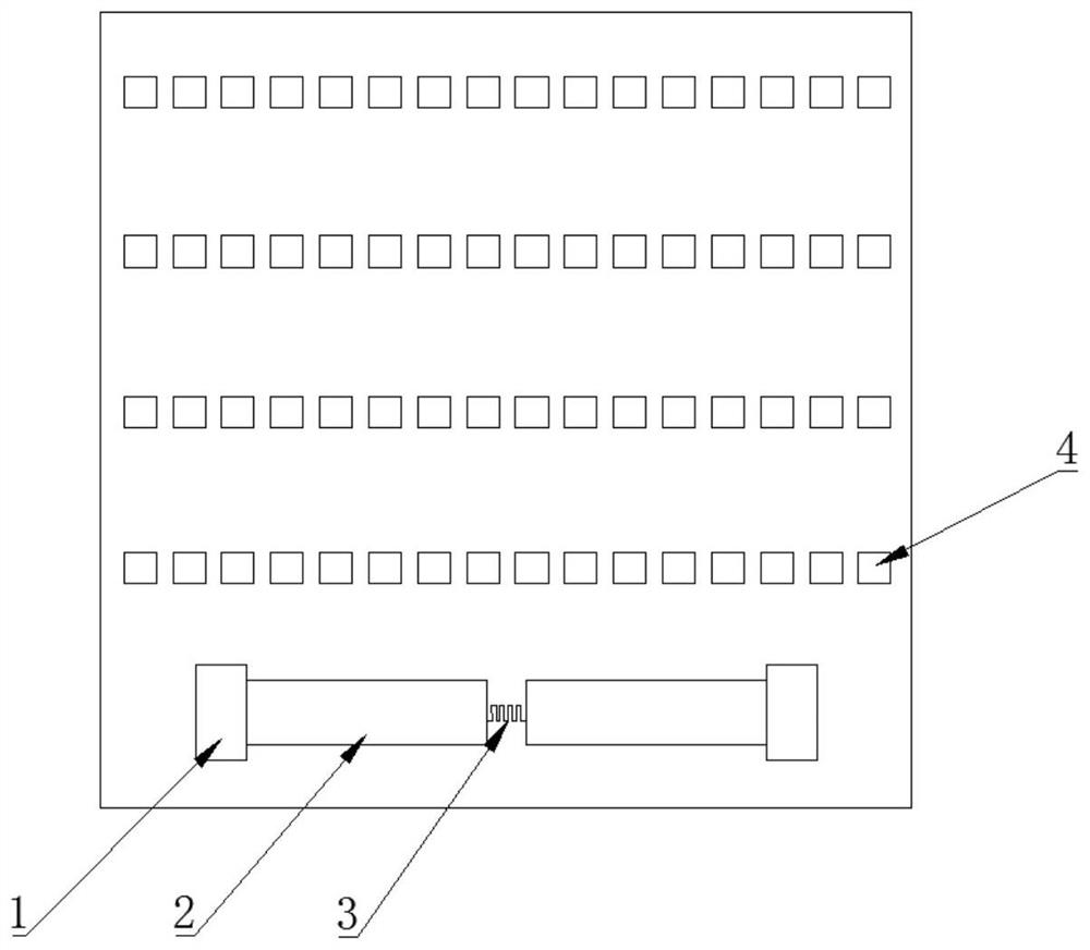
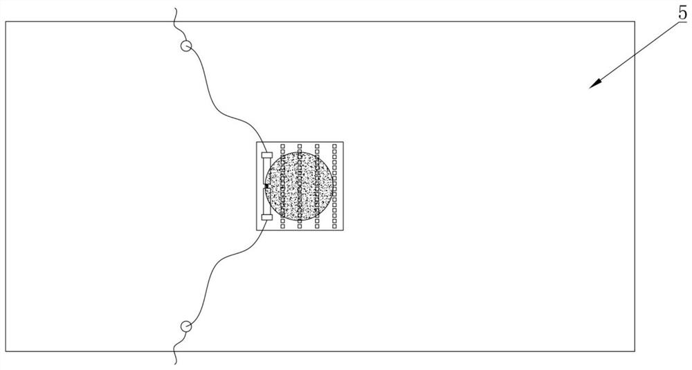
[0059] In this embodiment, the secondary excitation self-destruct chip based on the array channel is as follows: Figure 1-3 shown. The secondary excitation self-destruction chip based on the array hole includes a base layer and a self-destruction structure.

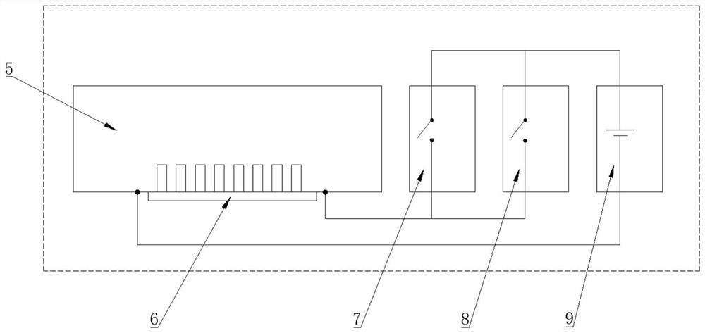
[0060] The base layer is the target chip 5 .

[0061] The self-destruct structure is arranged on the back of the target chip 5 and includes a heating circuit, a plurality of holes 4 , an energetic material layer 6 , a photosensitive switch 7 , a force sensitive switch 8 and a power supply 9 . The holes 4 are arranged in an array in the area to be damaged on the target chip 5 , and the energetic material layer 6 covers the heating area of ​​the heating circuit and part of the hole array area.

[0062] The heating circuit includes an electrode pad 1, two metal wires 2 and a heating wire 3. The electrode pad 1 includes a positive electrode pad and a negative electrode pad, and the positive electrode pad and the negative e...

Embodiment 2

[0067] The following describes the preparation method of the secondary excitation self-destruct chip based on the arrayed channel provided in Example 1. In this example, the base material of the substrate is a silicon single crystal substrate, and the specific steps are as follows:

[0068] S1. Provide a silicon single crystal substrate, prepare an insulating layer on the back of the silicon single crystal substrate, and deposit a metal conductive layer on the surface of the insulating layer:

[0069] S11. Cleaning preparation: clean the silicon single crystal substrate, ultrasonically clean the silicon single crystal substrate with acetone, ethanol, and deionized water for 10 minutes respectively, take it out, dehydrate and dry it under nitrogen atmosphere at 300°C, and set aside;

[0070] S12. Oxide film preparation: After the treatment in step S11, place the silicon single crystal substrate vertically on the sample holder, push it into the thermal oxidation furnace, close th...


PUM

PropertyMeasurementUnit
widthaaaaaaaaaa
lengthaaaaaaaaaa
thicknessaaaaaaaaaa

Abstract

The invention discloses a two-stage excitation self-destruction chip based on array type pore channels, and a preparation method thereof. The two-stage excitation self-destruction chip comprises a substrate layer and a self-destruction structure; the substrate layer is a target chip; and the self-destruction structure is arranged on the back face of the target chip and comprises a heating circuit, a plurality of hole channels and an energetic material layer, the hole channels are arranged in a to-be-damaged area on the target chip in an array mode, the energetic material layer covers a heating area of the heating circuit and a hole channel array area, and the heating circuit is connected in series in a circuit loop formed by an external control unit and a power supply unit. The self-destruction chip can be prepared by a conventional chip preparation process. According to the self-destruction chip, a weak current excitation-chemical burning explosion two-stage excitation structure is adopted, three-dimensional structures such as array type hole channels and deep holes are arranged on a semiconductor substrate to reduce the strength of the substrate, so that comminuted damage of a target chip is achieved; and thorough destruction of the target chip under the low-power-consumption working condition is achieved through two technical means, the information security of the chip is ensured.

Description

technical field [0001] The invention belongs to information security and semiconductor devices, and relates to a structural design and a preparation method that can be integrated with a core chip or a micro-electromechanical device (MEMS) and has a self-destruct function. Chip and its preparation method. Background technique [0002] With the rapid development of modern information technology, various semiconductor devices based on semiconductor materials such as silicon and gallium nitride have been widely used in information acquisition, analysis, storage, and transmission in the military and civilian fields. With a large amount of core data. If the information terminal equipment is lost or stolen, the important information stored in the memory chip may be stolen and leaked. Therefore, it is necessary to add a self-destruct function to memory chips and other important chips during product planning and design. Ensure that the core chip can be destroyed in an emergency to ...

Claims


Application Information

Patent Timeline
Patent Type & Authority Applications(China)
IPC IPC(8): H01L23/00
CPCH01L23/573
Inventor 任丁邵梦凡刘波昂然林黎蔚
Owner SICHUAN UNIV
Why Eureka
Try Eureka