Filter disc for X-ray and soft X-ray wave bands and preparation method thereof
An X-ray and filter technology, applied in the field of X-ray and soft X-ray filters and their preparation, can solve the problems of high cost and complicated operation
- Summary
- Abstract
- Description
- Claims
- Application Information
AI Technical Summary
Problems solved by technology
Method used
Image
Examples
preparation example Construction
[0032] The present invention also provides a preparation method of the filter sheet described in the above technical solution, comprising the following steps:
[0033] A polyimide film is deposited on the polished surface of the silicon wafer by thermal evaporation, and then the non-polished surface of the silicon wafer is etched to expose the polyimide film, and then magnetron sputtering is used on the exposed surface. The surface of the polyimide film is followed by Sc layer and B 4 Coating of layer C to obtain the filter disc.
[0034] In the present invention, the magnetron sputtering coating preferably uses Sc target and B 4 C target, the sputtering power of the Sc target is preferably 60W, the B 4 The sputtering power of the C target is preferably 120W.
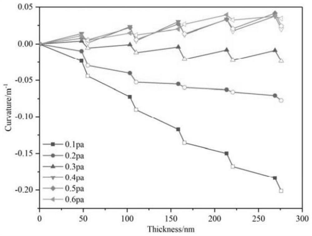
[0035] In the present invention, the sputtering pressure of the magnetron sputtering coating is preferably 0.1-0.5Pa, more preferably 0.3-0.4Pa.
[0036] In the present invention, the background vacuum degree of the...
Embodiment 1
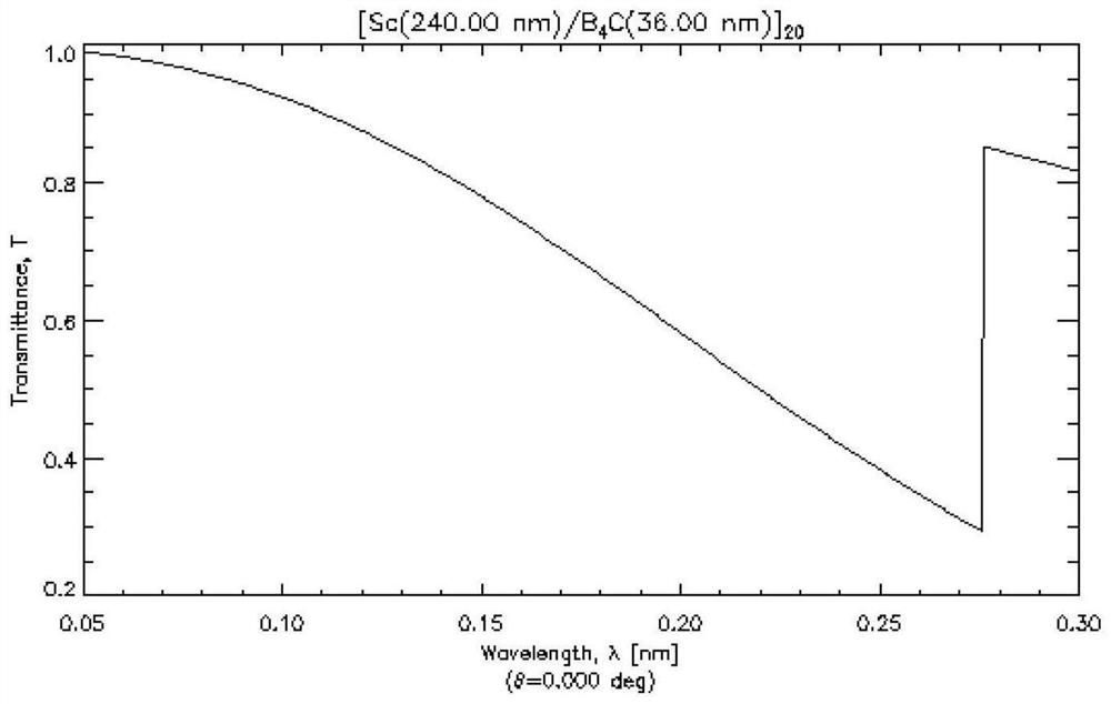
[0043] A filter for X-ray and soft X-ray bands, comprising alternately stacked Sc layers and B 4 C layer, the number of cycles of alternate lamination is 20 times, the thickness of each layer of Sc layer is 240nm, each layer of B 4 The thickness of layer C is 36nm, and the filter also includes a polyimide film as a self-supporting film with a thickness of 1.7 μm.
[0044] The preparation method is as follows:
[0045] First, a layer of PI film with a thickness of 1.7 μm is deposited on the polished surface of the silicon wafer by thermal evaporation, and the non-polished surface of the silicon wafer is first etched to form a circular groove area of the required filter size. The diameter of the circular groove is 10 mm. The silicon in the circular groove is completely etched, and the PI film is exposed, and then the Sc / B film is deposited by magnetron sputtering. 4 C (Sc: 4.8 μm, B 4 C: 0.72 μm) deposited on PI film, Sc / B 4 The C film is divided into 20 cycles in total, and...
Embodiment 2
[0051] A filter for X-ray and soft X-ray bands is the same as in Embodiment 1.
[0052] The preparation method is as follows:
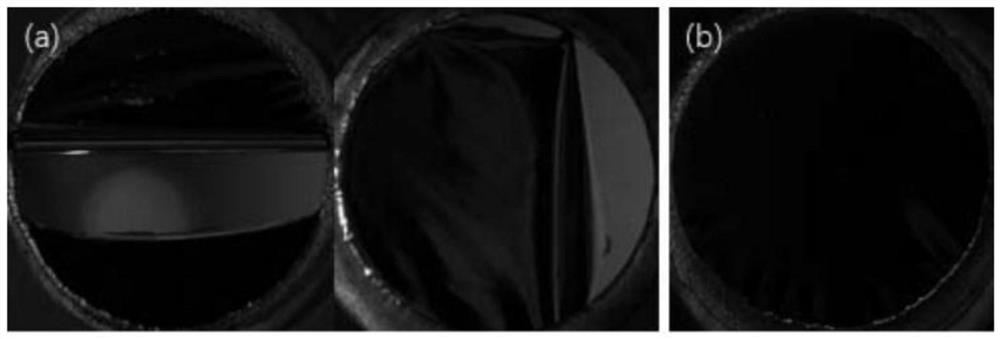
[0053] Etch a circular groove area with a diameter of 5mm on the non-polished surface of the silicon wafer, and then expose the PI film, and then sputter-deposit Sc / B on the PI film 4 C, the whole process is divided into 20 cycles, Sc target and B in the process of magnetron sputtering 4 The sputtering power of the C target is 60W and 100W, and the spacer thickness is 48nm and 7.2nm, respectively, using this method to deposit Sc / B on the PI film 4 At C, the PI film rupture was significantly reduced, and the PI film and Sc / B 4 The yield of C composite filter is greatly improved. The advantage of this preparation method is that the circular groove-shaped area etched on the silicon wafer is small, and the Sc / B is deposited on the PI film. 4 C, the stress on the PI film is not enough to cause it to rupture, and more heat generated during the sputterin...
PUM
| Property | Measurement | Unit |
|---|---|---|
| thickness | aaaaa | aaaaa |
| thickness | aaaaa | aaaaa |
| thickness | aaaaa | aaaaa |
Abstract
Description
Claims
Application Information


