Printing ink for PCB of LED display screen, preparation method of LED display module using printing ink and LED display screen

A technology of LED display screen and PCB board, which is applied in the direction of printing ink, photographic plate-making process of patterned surface, and photosensitive material used in optical mechanical equipment, etc. advanced questions

Pending Publication Date: 2021-05-28
HUIZHOU ABSEN OPTOELECTRONIC CO LTD
View PDF3 Cites 3 Cited by
  • Summary
  • Abstract
  • Description
  • Claims
  • Application Information

AI Technical Summary

Problems solved by technology

Therefore, it is necessary to provide a kind of matting solder resist ink with low gloss and high absorpti

Method used


Image

  • Printing ink for PCB of LED display screen, preparation method of LED display module using printing ink and LED display screen
  • Printing ink for PCB of LED display screen, preparation method of LED display module using printing ink and LED display screen
  • Printing ink for PCB of LED display screen, preparation method of LED display module using printing ink and LED display screen

Examples


Example Embodiment

[0055] Correspondingly, the embodiment of the present application also provides a method for preparing an LED display module using the above-mentioned matting solder resist ink, including the following steps:

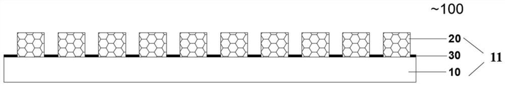
[0056] S100, coating or printing the matt solder resist ink obtained by mixing the first component and the second component on the first surface of the PCB, and then pre-baking, exposure treatment, development treatment, and post-baking, Forming a patterned matte solder resist ink layer;

[0057] S200, mounting a plurality of LED lamp beads on the area of ​​the first surface not covered by the matting solder resist ink layer to obtain an LED display module.

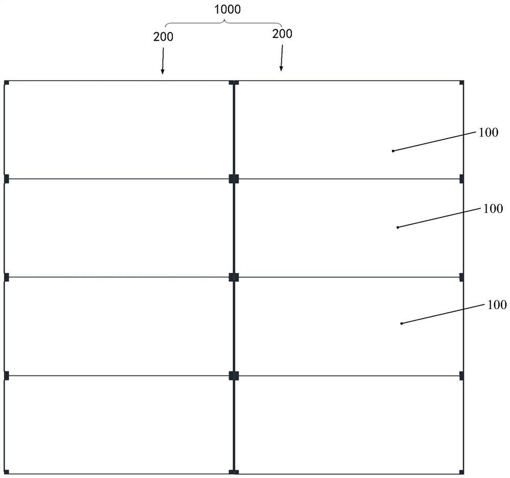
[0058] In step S100, the first surface of the PCB board is the side surface of the PCB board to be mounted with LED lamp beads. The above-mentioned coating methods may include brush coating, spray coating, doctor blade coating or spin coating, etc., and the specific printing method may be screen printing, and its ...

Example Embodiment

[0067] Example 1

[0068] A kind of matting solder resist ink for LED display PCB board, comprises the first component and the second component that store separately, and described first component comprises each raw material of following mass percentage content:

[0069] Oligomer (specifically modified o-methyl novolak epoxy acrylic resin, viscosity at 60°C is 2500mPa·s): 35%;

[0070] Photoinitiator: 10%, specifically 7% of 2-methyl-1-(4-methylthiophenyl)-2-morpholine-1-propanone and 3% of 2-isopropylthioxanthone ;

[0071] Nano black filler (specifically carbon microspheres with a particle size of 30nm): 10%;

[0072] Matting agent (specifically fumed silica, secondary particle size is 10 μm): 18%;

[0073] Coupling agent (specifically aminopropyltriethoxysilane): 2%;

[0074] DBE solvent: 25%;

[0075] Described second component comprises each raw material of following mass percentage content:

[0076] Epoxy resin (specifically novolac type epoxy resin, the viscosity ...

Example Embodiment

[0087] Example 2

[0088] A kind of matting solder resist ink for LED display PCB board, comprises the first component and the second component that store separately, and described first component comprises each raw material of following mass percentage content:

[0089] Oligomer (specifically novolac epoxy acrylic resin, viscosity at 60°C is 3000mPa·s): 33%;

[0090] Photoinitiator 10%, specifically 7% of 2-methyl-1-(4-methylthiophenyl)-2-morpholine-1-propanone and 3% of 2-isopropylthioxanthone) ;

[0091] Nano black filler (specifically carbon microspheres with a particle size of 30nm): 10%;

[0092] Matting agent (specifically fumed silica, secondary particle size is 10 μm): 20%;

[0093] Coupling agent (specifically aminopropyltriethoxysilane): 2%;

[0094] DBE solvent: 25%;

[0095] Described second component comprises each raw material of following mass percentage content:

[0096] Epoxy resin (specifically bisphenol F type epoxy resin, the viscosity at 25°C is 150...


PUM

PropertyMeasurementUnit
Thicknessaaaaaaaaaa
Viscosityaaaaaaaaaa
Particle sizeaaaaaaaaaa

Abstract

The invention provides extinction solder resist ink for a PCB of an LED display screen, which comprises a first component and a second component, wherein the first component comprises 20%-50% of oligomer, 0.5%-15% of photoinitiator, 5%-15% of nano black filler, 10%-30% of matting agent, 0.2%-2% of coupling agent and 10%-30% of solvent; and the second component comprises 20%-40% of epoxy resin, 5%-40% of a functional monomer, 10%-20% of a delustering agent, 0.2%-2% of a coupling agent and 5%-15% of a solvent; the first component and the second component are stored separately and are mixed when in use. The extinction solder resist ink has good solder resist performance and excellent extinction performance, and can effectively improve the problem of inconsistent ink color when the LED display screen is black. The invention further provides a preparation method of an LED display module adopting the extinction solder resist ink and an LED display screen.

Description

technical field [0001] The application relates to the technical field of LED display screens, in particular to an ink for LED display PCB boards, a method for preparing an LED display module using the ink, and a display screen. Background technique [0002] Light emitting diode (light emitting diode, LED) display has the advantages of high luminous brightness, high luminous efficiency, bright color, high contrast, wide operating temperature range, short response time, low energy consumption, etc., and is widely used in the display field, such as the more common Securities trading and financial information display, airport flight dynamic information display, port and station passenger guidance information display, stadium information display, road traffic information display, power dispatching and vehicle dynamic tracking and other dispatching command center information display, shopping malls and other services Display of business publicity information and advertising media ...

Claims


Application Information

Patent Timeline
IPC IPC(8): C09D11/101C09D11/03G03F7/004G03F7/027G09F9/33
CPCC09D11/101C09D11/03G03F7/004G03F7/027G09F9/33
Inventor 李小明徐勋明夏建平甘志勇吴隆云
Owner HUIZHOU ABSEN OPTOELECTRONIC CO LTD
Why Eureka
Try Eureka