Physical vapor deposition of piezoelectric films

A physical vapor deposition, piezoelectric layer technology, applied in electrical components, piezoelectric/electrostrictive/magnetostrictive devices, circuits, etc., to reduce overheating, improve downtime, and excellent piezoelectric performance.

Pending Publication Date: 2021-05-28
APPLIED MATERIALS INC
View PDF0 Cites 1 Cited by
  • Summary
  • Abstract
  • Description
  • Claims
  • Application Information

AI Technical Summary

Problems solved by technology

However, large-area thin-film deposition of relaxed-PT layers in a commercially viable manner has not yet been achieved

Method used


Image

  • Physical vapor deposition of piezoelectric films
  • Physical vapor deposition of piezoelectric films
  • Physical vapor deposition of piezoelectric films

Examples


Embodiment Construction

[0014] Fabrication of piezoelectric layers from bulk crystals and deposition of piezoelectric layers using sol-gel techniques are slow processes that do not favor implementation in semiconductor fabrication plants. Bulk crystals require processing in conventional machine shops. Not only is this expensive, but it limits the ability to integrate piezoelectric layers into devices. The sol-gel process requires multiple rounds of deposition and curing, making the process time-consuming. Therefore, it is desirable to deposit piezoelectric materials by physical vapor deposition processes such as sputtering.

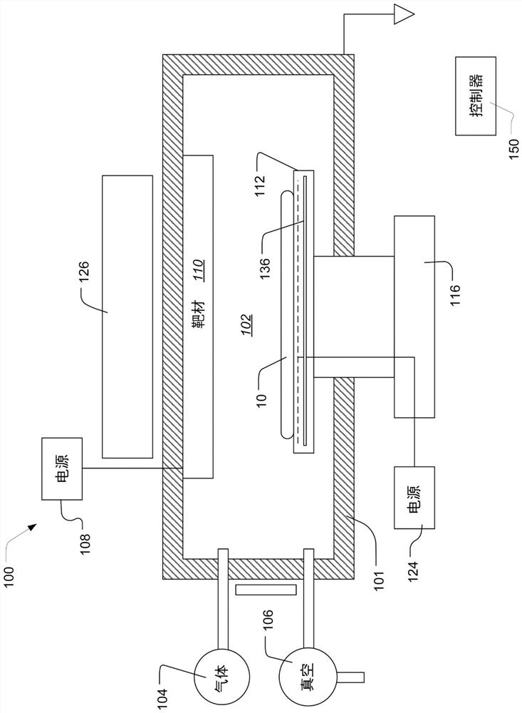
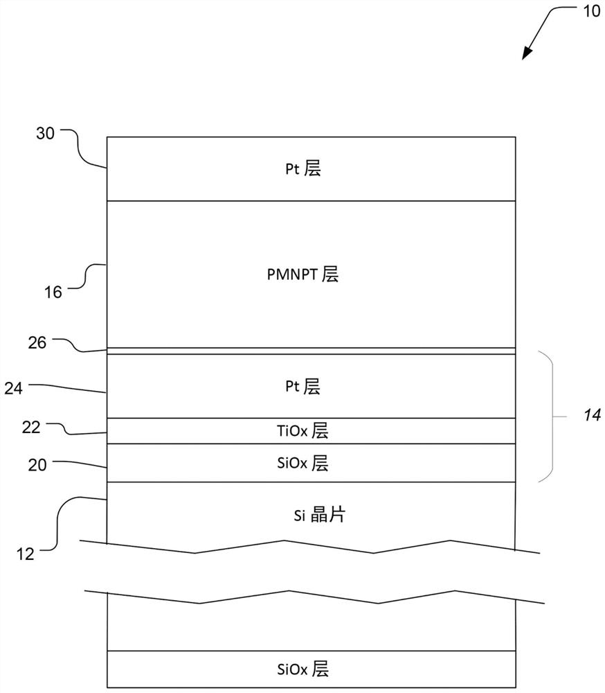
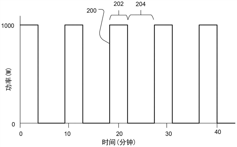
[0015] Fabricating thin films of piezoelectric materials on large-area semiconductor wafers, such as silicon wafers, by physical vapor deposition (PVD) is challenging. For PVD of piezoelectric materials such as PZT or Relax-PT, the target material used in the sputtering process is a ceramic material. However, targets used in chambers may crack or suffer other forms of damage....


PUM

PropertyMeasurementUnit
thicknessaaaaaaaaaa
thicknessaaaaaaaaaa
thicknessaaaaaaaaaa

Abstract

The invention relates to a method for manufacturing a piezoelectric layer. The method comprises: depositing a piezoelectric material of a first crystalline phase onto a substrate by physical vapor deposition while maintaining the substrate at a temperature below 400 DEG C; and thermally annealing the substrate at a temperature above 500 DEG C to convert the piezoelectric material into a second crystalline phase. The physical vapor deposition comprises sputtering from a target in a plasma deposition chamber.

Description

technical field [0001] This invention relates to the fabrication of piezoelectric devices and, more particularly, to physical vapor deposition of piezoelectric films. Background technique [0002] Piezoelectric materials have been used for decades in various technologies such as inkjet printing, medical ultrasound, and gyroscopes. Traditionally, piezoelectric layers have been fabricated by fabricating the piezoelectric material in the form of bulk crystals and then processing the material to the desired thickness, or by depositing the layers using sol-gel techniques. Lead zirconate titanate (PZT), usually Pb[Zr x Ti 1-x ]O 3 form, is a commonly used piezoelectric material. Sputtering of PZT has been proposed. [0003] Recently, relaxor-lead titanate (relax-PT), such as (1-X)[Pb(Mg 1 / 3 Nb 2 / 3 )O 3 ]-X[PbTiO 3 ](PMN-PT), (1-X)[Pb(Y 1 / 3 Nb 2 / 3 )O 3 ]-X[PbTiO 3 ](PYN-PT), (1-X)[Pb(Zr 1 / 3 Nb 2 / 3 )O 3 ]-X[PbTiO 3 ](PZN-PT), (1-X)[Pb(In 1 / 3 Nb 2 / 3 )O 3 ]-X[PbTiO...

Claims


Application Information

Patent Timeline
Patent Type & Authority Applications(China)
IPC IPC(8): C23C14/35C23C14/10C23C14/08
CPCC23C14/352C23C14/10C23C14/083C23C14/088C23C14/5806C23C14/3485C23C14/541C23C14/024H10N30/10516H10N30/8548H10N30/079H10N30/076C23C14/351C23C14/06C23C14/54H10N30/877
Inventor 阿比吉特·拉克斯曼·桑格尔维杰·班·夏尔马安库尔·凯达姆巴拉特瓦·罗摩克里希南维斯韦斯瓦伦·西瓦拉玛克里施南薛元
Owner APPLIED MATERIALS INC
Why Eureka
Try Eureka