Perovskite HJT laminated tile solar cell module and preparation method thereof
A solar cell and perovskite technology, which is applied in the manufacture of electrical components, electrical solid devices, semiconductor/solid devices, etc., can solve the problems of large power loss in photoelectric conversion, uneven current collection of photovoltaic modules, etc., and reduce heat loss , Quick and convenient preparation, less demanding effect
- Summary
- Abstract
- Description
- Claims
- Application Information
AI Technical Summary
Problems solved by technology
Method used
Image
Examples
Embodiment 1
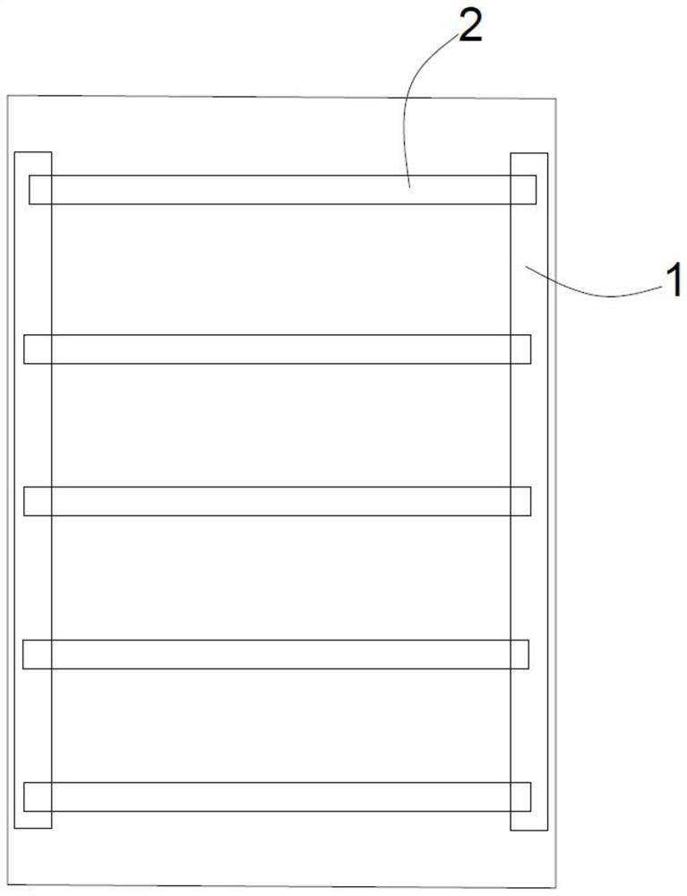
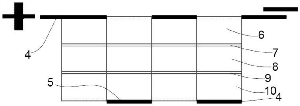
[0036] This embodiment proposes a perovskite HJT stacked shingled solar cell assembly, which includes several cell modules, and the cell modules are in a forward structure. Specifically, the cell modules include rear grid lines 4 arranged in sequence, The back gate line 4 can be any one of Ag, Al or Au, the thickness is about 100-6000nm, the gate line width is 30um, and includes at least two groups of main gates 1, and several main gates 1 are arranged between them. Auxiliary grid 2,
[0037] The thickness of the HJT battery layer 6 is generally controlled at about 180 μm, and the top of the HJT battery layer 6 in the forward structure is the P side;
[0038] Conductive base layer 7, described conductive base layer 7 comprises any one in FTO conductive glass, ITO conductive glass, FTO conductive plastic, ITO conductive plastic, the thickness of described FTO conductive glass or FTO conductive plastic is 450nm~500nm, so The thickness of the ITO conductive glass or ITO conducti...
Embodiment 2
[0047] This embodiment discloses a reverse structure, including several battery chip modules, and the battery chip modules include rear gate lines 4, HJT battery layer 6, conductive base layer 7, hole transport layer 10, and perovskite layer arranged in sequence. 9. The electron transport layer 8 and the front grid 5, the top of the HJT battery layer 6 is the N side, the front grid 5 and the back grid include at least two groups of main grids 1, and the main grids 1 are arranged in an arrangement There are several sub-grids 2; the main grids 1 between adjacent cells are stacked and connected by conductive glue 3. The back grid line 4 can be any one of Ag, Al or Au, the thickness is about 100-6000nm, the width of the grid line is 30um, and includes at least two groups of main grids 1, and several main grids 1 are arranged between them. Auxiliary grid 2,
[0048] The thickness of the HJT battery layer 6 is generally controlled at about 180 μm, and the top of the HJT battery lay...
PUM
| Property | Measurement | Unit |
|---|---|---|
| Thickness | aaaaa | aaaaa |
| Thickness | aaaaa | aaaaa |
| Thickness | aaaaa | aaaaa |
Abstract
Description
Claims
Application Information
 - R&D Engineer
- R&D Manager
- IP Professional
- Industry Leading Data Capabilities
- Powerful AI technology
- Patent DNA Extraction
Browse by: Latest US Patents, China's latest patents, Technical Efficacy Thesaurus, Application Domain, Technology Topic, Popular Technical Reports.
© 2024 PatSnap. All rights reserved.Legal|Privacy policy|Modern Slavery Act Transparency Statement|Sitemap|About US| Contact US: help@patsnap.com


