

Complex-surface thin film transistor and self-aligned electrofluid conformal photoetching manufacturing method
A technology of thin-film transistors and complex curved surfaces, which is applied in semiconductor/solid-state device manufacturing, circuits, electrical components, etc., to achieve the effects of avoiding erosion, improving resolution, improving electrical stability and service life
- Summary
- Abstract
- Description
- Claims
- Application Information
AI Technical Summary
Problems solved by technology
Method used
Image

Examples
Embodiment Construction
[0036] In order to make the object, technical solution and advantages of the present invention clearer, the present invention will be further described in detail below in conjunction with the accompanying drawings and embodiments. It should be understood that the specific embodiments described here are only used to explain the present invention, not to limit the present invention. In addition, the technical features involved in the various embodiments of the present invention described below can be combined with each other as long as they do not constitute a conflict with each other.
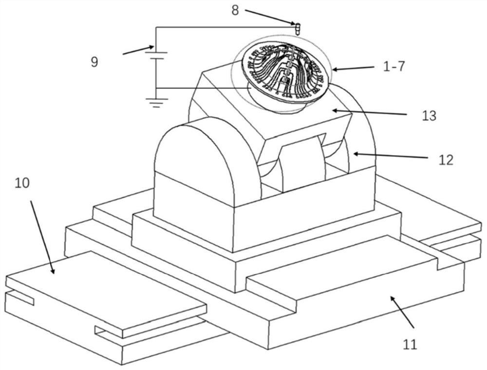
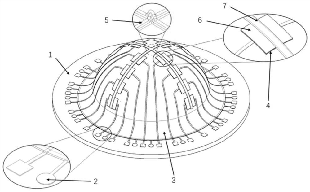
[0037] see figure 1 , figure 2 , Figure 4 and Figure 5 , the present invention provides a self-aligned electrofluid conformal lithography manufacturing method of complex curved surface thin film transistors, the preparation method is a self-aligned electrofluid conformal lithography manufacturing method, which includes the following steps:
[0038]Step 1, preparing a three-dimensional cur...
PUM
 Abstract
Description
Claims
Application Information