Shape-controllable silicon dioxide nano array and preparation method and application thereof
What is AI technical title?
AI technical title is built by Patsnap AI team. It summarizes the technical point description of the patent document.
A silicon dioxide and nanoarray technology, applied in the field of nanomaterials, can solve the problems of complex processing process and difficult to control surface structure, etc.
Active Publication Date: 2021-06-11
FUDAN UNIV
View PDF7 Cites 0 Cited by
Summary
Abstract
Description
Claims
Application Information
AI Technical Summary
This helps you quickly interpret patents by identifying the three key elements:
Problems solved by technology
Method used
Benefits of technology
Problems solved by technology
[0002] The nano-biological interaction is affected by the surface structure of the substrate, but some existing methods (such as chemical etching process, electrochemical deposition, chemical vapor deposition), the processing process is often complicated, and it is difficult to precisely control the surface structure at the nanoscale
Method used
Image
Click on the blue label to locate the original text in one second.
Reading with bidirectional positioning of images and text.
Examples
Embodiment 1
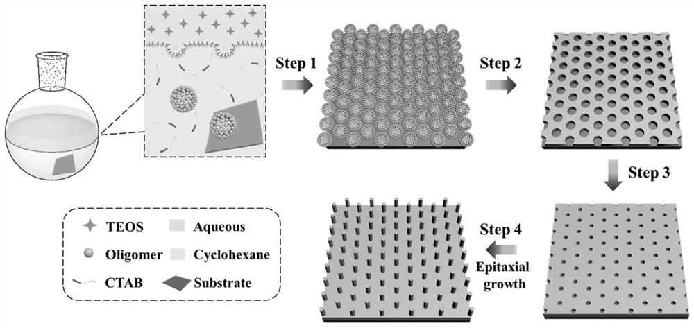
[0054] Growth of silica nanoarrays on silicon wafers:
[0055] (1) Dissolve 0.5 wt.% cetyltrimethylammonium bromide (CTAB) and 0.008 wt.% sodiumhydroxide in water in turn to obtain a clear solution, and control the temperature at 60 °C;
[0056] (2) Add silicon wafers and continue to stir at 60 °C;
[0057] (3) Add a mixed solution of cyclohexane and tetraethylorthosilicate (TEOS), and control the volume ratio of cyclohexane, TEOS and water to 6: 1.5: 10;
[0058] (4) Control the temperature at 60 °C and react for 48 h;
[0059] (5) After the reaction is over, take out the silicon wafer and wash it.
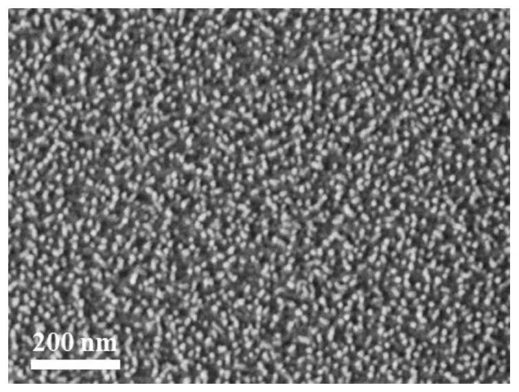
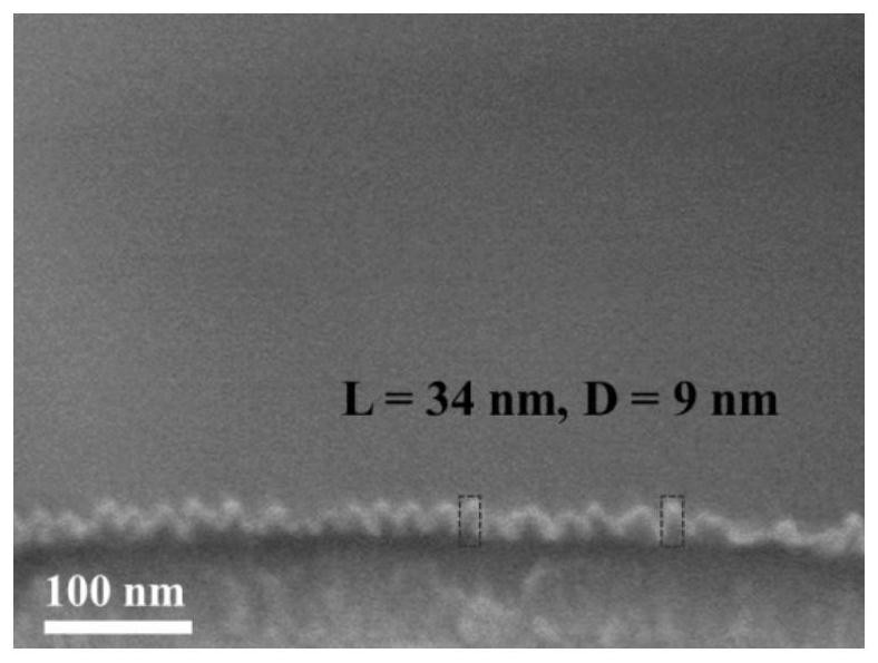
[0060] The silicon dioxide nanoarray layer grown on the silicon wafer was obtained, and the distribution density of the silicon dioxide nanoarray (spine) was 510 nanothorns / μm 2 , the average distance between adjacent silica nanopeaks is 46 nm. like Figure 4 , Figure 5 shown.
Embodiment 2
[0062] Growth of silica nanoarrays on glass rods:
[0063] (1) Dissolve 2 wt.% cetyltrimethylammonium bromide (CTAB) and 0.01 wt.% sodiumhydroxide in water in turn to obtain a clear solution, and control the temperature at 60 °C;
[0064] (2) Add a glass rod and continue stirring at 60 °C;
[0065] (3) Add a mixed solution of cyclohexane and tetraethylorthosilicate (TEOS), and control the volume ratio of cyclohexane, TEOS and water to 6: 1.5: 10;
[0066] (4) Control the temperature at 60 °C and react for 48 h;
[0067] (5) After the reaction, the glass rod was taken out and washed to obtain a silicon dioxide nano-array layer grown on the glass rod. like Figure 6 , Figure 7 shown.
Embodiment 3
[0069] Growth of silica nanoarrays on glass tubes:
[0070] (1) Dissolve 2 wt.% cetyltrimethylammonium bromide (CTAB) and 0.01 wt.% sodiumhydroxide in water in turn to obtain a clear solution, and control the temperature at 60 °C;
[0071] (2) Add the glass tube and continue stirring at 60 °C;
[0072] (3) Add a mixed solution of cyclohexane and tetraethylorthosilicate (TEOS), and control the volume ratio of cyclohexane, TEOS and water to 6: 1.5: 10;
[0073] (4) Control the temperature at 60 °C and react for 48 h;
[0074] (5) After the reaction, the glass tube was taken out and washed to obtain a silicon dioxide nano-array layer grown on the glass tube. like Figure 8 , Figure 9 shown.
PUM
Property
Measurement
Unit
height
aaaaa
aaaaa
thickness
aaaaa
aaaaa
length
aaaaa
aaaaa
Abstract
The invention belongs to the technical field of nano materials, and particularly relates to a shape-controllable silicon dioxide nano array and a preparation method and application thereof. According to the silicon dioxide nano array, the array height is 8-46 nm, and the distribution density is 210-3100 / mu m < 2 >. The preparation method of the nano array comprises the following steps: forming a silicon nano array on the surface of a substrate by adopting an oil / water double-phase single micelle epitaxial growth method and taking CTAB as a structure-directing agent, TEOS as a precursor and NaOH as a catalyst; the substrate can be a glass sheet, a silicon wafer, a glass rod, a glass tube, a micro-fluidic chip and the like. The silicon dioxide nano array can endow the substrate with a rough surface structure, and the interaction between the substrate and tumor cells and the biological interface is enhanced. Compared with a substrate modified by a smooth silicon layer, the cell adhesion capacity is remarkably improved. The device formed by nesting the glass rod with the silicon dioxide nano array growing on the surface and the glass tube can be used for separating tumor cells from whole blood.
Description
technical field [0001] The invention belongs to the technical field of nanometer materials, and in particular relates to a silicon dioxide nanoarray with controllable shape, its preparation method and application. Background technique [0002] The nano-biological interaction is affected by the surface structure of the substrate, but some existing methods (such as chemical etching process, electrochemical deposition, chemical vapor deposition), the processing process is often complicated, and it is difficult to precisely control the surface structure at the nanoscale . [0003] Compared with smooth interfaces, substrates with nanotopographic interfaces, such as nanoarrays, nanofibers, etc., interact with cells differently. Previous studies have shown that surface nanostructures can significantly increase the contact frequency between substrates and cells (such as nano-scale microvilli, filopodia, surface receptors, etc.), thereby improving the adhesion efficiency of cells. ...
Claims
Application Information
Patent Timeline
Application Date:The date an application was filed.
Publication Date:The date a patent or application was officially published.
First Publication Date:The earliest publication date of a patent with the same application number.
Issue Date:Publication date of the patent grant document.
PCT Entry Date:The Entry date of PCT National Phase.
Estimated Expiry Date:The statutory expiry date of a patent right according to the Patent Law, and it is the longest term of protection that the patent right can achieve without the termination of the patent right due to other reasons(Term extension factor has been taken into account ).
Invalid Date:Actual expiry date is based on effective date or publication date of legal transaction data of invalid patent.

