GaN BASED LIGHT EMITTERS WITH BAND-EDGE ALIGNED CARRIER BLOCKING LAYERS

a technology of carrier blocking layer and gan, which is applied in the field of nitridesemiconductor based light emitting devices, can solve the problems of low efficiency of these devices, lower epitaxial quality, and higher thermal resistance, and achieve the effect of improving the capture efficiency of electrons

Active Publication Date: 2010-10-28
DR SAMALS LAB
View PDF2 Cites 30 Cited by
  • Summary
  • Abstract
  • Description
  • Claims
  • Application Information

AI Technical Summary

Benefits of technology

[0017]This invention allows enhancement of the capture efficiency of electrons and holes into the active QW of nitride-based light emitters such as laser diodes and LEDs.

Problems solved by technology

This results in low efficiency of these devices.
However, this leads to a lower epitaxial quality and a higher thermal resistance for aluminum content up to 50%.
Furthermore, to avoid a higher voltage drop and to keep the optical confinement factor constant, the aluminum content of the cladding layers also has to be raised, which further degrades the thermal and epitaxial quality.
However, in an undoped state, they increase the series resistance and generate an additional voltage drop due to their limited electronic transport properties (Weidmann et al.
Since high optical output power demands minimized thermal and electrical resistance, increasing the quantum-well barrier height do not seem to be quite viable.
However, due to lighter mass and host of other reasons such as spontaneous and peizo-electric field in the well region, electrons tend to overflow the quantum wells and thus recombine with holes non-radiatively outside the wells.

Method used


Image

  • GaN BASED LIGHT EMITTERS WITH BAND-EDGE ALIGNED CARRIER BLOCKING LAYERS
  • GaN BASED LIGHT EMITTERS WITH BAND-EDGE ALIGNED CARRIER BLOCKING LAYERS
  • GaN BASED LIGHT EMITTERS WITH BAND-EDGE ALIGNED CARRIER BLOCKING LAYERS

Examples


Embodiment Construction

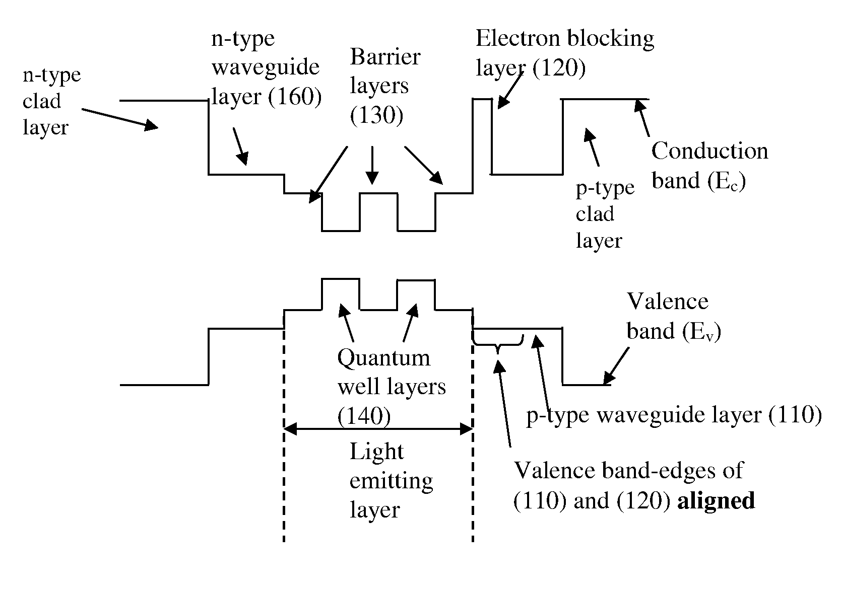
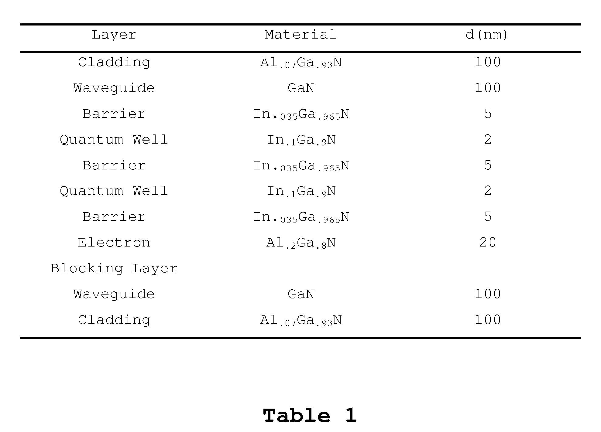
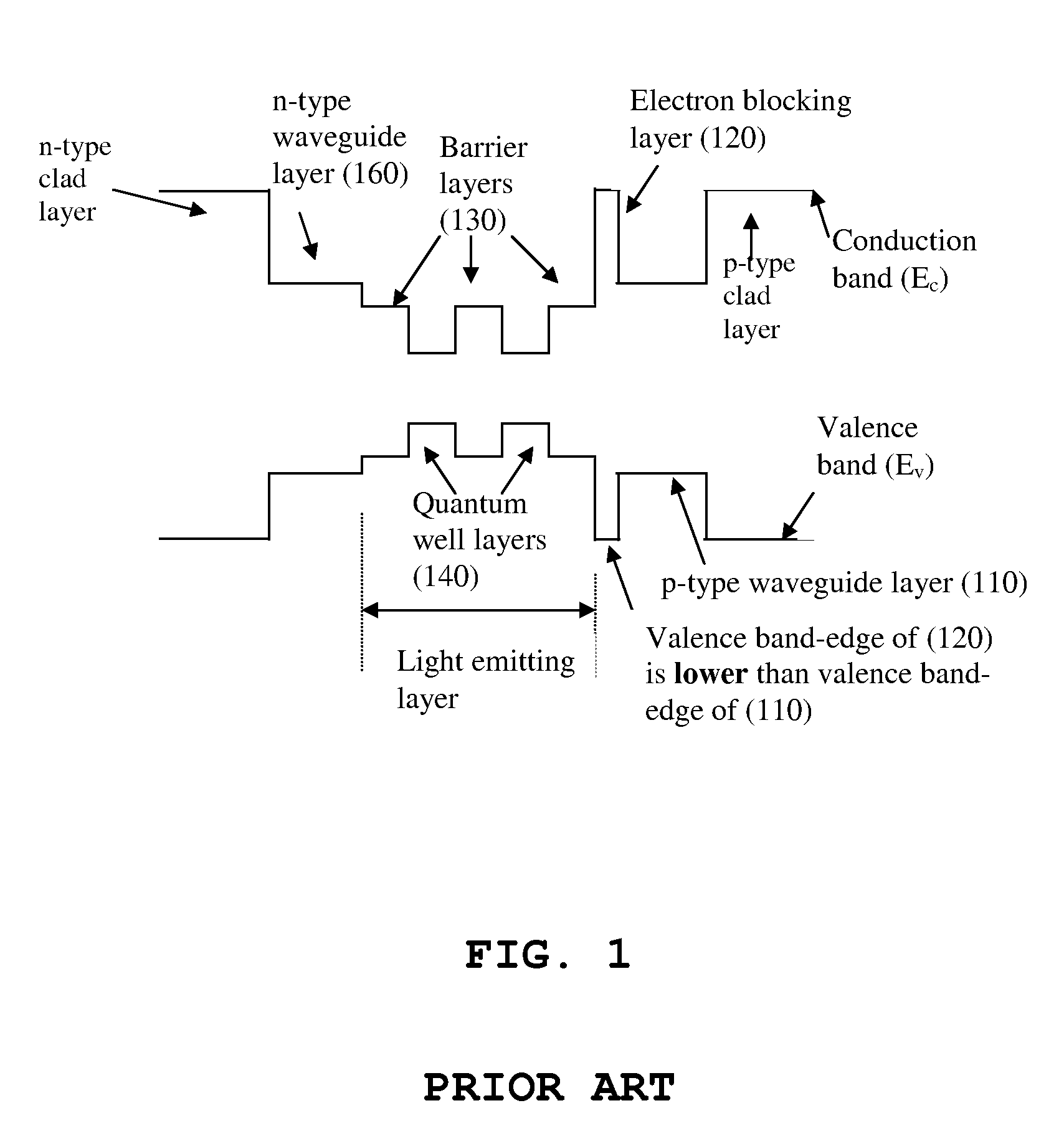
[0059]In case of GaN based system, as briefly discussed earlier, AlGaN or InAlGaN layers are typically used as electron blocking layers. However, these layers also block holes in the valence band from reaching the QW, which leads to lowering of internal quantum efficiency in the QW. Moreover, hole-blocking by electron-blocking layer naturally becomes more severe with increasing Al-content in the blocking layer as increasing Al content increases both conduction and valence band offset relative to barrier or waveguide layer. Typical Al content in AlGaN electron blocking layer is around 0.2. The simulated energy band diagram of a typical customary structure (Chen et al. Journal of Lightwave Technology No. 3 Vol. 26 2008) is shown in FIG. 5. Constraints of not choosing higher Al-containing electron blocking layers lead to efficiency-drooping and lower temperature performance due to carrier overflow and non-radiative recombination, which becomes much more severe at higher current injecti...


PUM


Abstract

Band-edge aligned carrier blocking layers are introduced into wurtzite or zinc blende Gallium Nitride based diode laser and LEDs in order to prevent thermionic emission and the overflow of carriers at elevated operating temperatures. These blocking layers are located in the direct vicinity of the active zone of the light emitter, and are designed with material composition such that one of the band-edges of the layers is, either partially or fully, aligned with that of adjacent barrier or waveguide layer. This invention proposes GaN based QW structure with a AlGaN(AsPSb) electron-blocking layer on the p-side of quantum well and (InGa)AlN as hole-blocking layer.

Description

BACKGROUND OF THE INVENTION[0001]1. Field of the Invention[0002]This invention relates to light emitters, and more particularly, to nitride-semiconductor based light emitting devices with high power, high luminous efficiency and optical apparatus using the same.[0003]2. Description of the Related Art[0004]Nitride based semiconductor materials have drawn tremendous attention during last decade due to its enormous potential to be utilized in white lighting and high-power semiconductor devices. In a nitride semiconductor light emitting device, InGaN is often used for a quantum well (QW) layer included in its light emitting layer and it emits a wide range of colors from blue to orange just by adjusting the In content in InGaN QW. In recent years, blue, green and violet semiconductor light emitting diodes (LED) and lasers have been developed utilizing the characteristics of the nitride semiconductor light emitting devices.[0005]For light generation in semiconductor lasers and LEDs, radia...

Claims


Application Information

Patent Timeline
Patent Type & Authority Applications(United States)
IPC IPC(8): H01L29/06
CPCB82Y20/00H01L33/06H01S5/34333H01L33/32H01L33/16
Inventor SAMAL, ASHMEET K.
Owner DR SAMALS LAB
Why Eureka
Try Eureka