Deep ultraviolet LED and manufacturing method thereof

A manufacturing method, deep ultraviolet technology, applied in the direction of semiconductor devices, electrical components, circuits, etc., can solve the problems of hole injection influence, reduction of deep ultraviolet LED luminous efficiency, hole carrier activation efficiency and concentration reduction, etc., to achieve Improve luminous efficiency and improve the effect of spatial wave function overlap

Active Publication Date: 2021-06-11
XIAMEN CHANGELIGHT CO LTD
View PDF9 Cites 2 Cited by
  • Summary
  • Abstract
  • Description
  • Claims
  • Application Information

AI Technical Summary

Problems solved by technology

[0008] However, with the gradual shortening of the wavelength of the deep ultraviolet LED, the Al composition of the quantum well gradually increases, that is, the Al composition of the electron blocking layer gradually increases, so the electron blocking layer effectively blocks electrons to prevent electron overflow. The injection of holes also adversely affects the
[0009] Specifically, in the electron blocking layer of AlGaN or AlN material, the acceptor impurity energy level is deeper than that of GaN, and with the increase of Al composition, the forbidden band width of AlGaN material increases, the acceptor energy level continues to deepen, and the activation energy Continuously increasing, leading to a decrease in the activation efficiency and concentration of hole carriers, thereby reducing the luminous efficiency of deep ultraviolet LEDs

Method used


Image

  • Deep ultraviolet LED and manufacturing method thereof
  • Deep ultraviolet LED and manufacturing method thereof
  • Deep ultraviolet LED and manufacturing method thereof

Examples


Embodiment Construction

[0045] The following will clearly and completely describe the technical solutions in the embodiments of the present invention with reference to the accompanying drawings in the embodiments of the present invention. Obviously, the described embodiments are only some, not all, embodiments of the present invention. Based on the embodiments of the present invention, all other embodiments obtained by persons of ordinary skill in the art without making creative efforts belong to the protection scope of the present invention.

[0046] In order to make the above objects, features and advantages of the present invention more comprehensible, the present invention will be further described in detail below in conjunction with the accompanying drawings and specific embodiments.

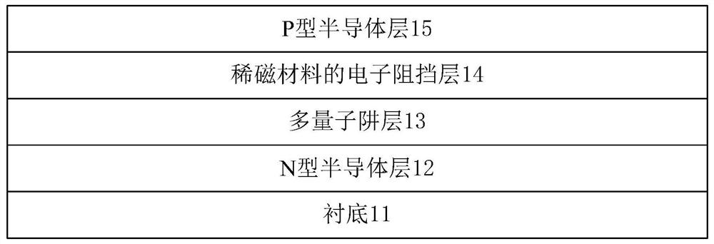
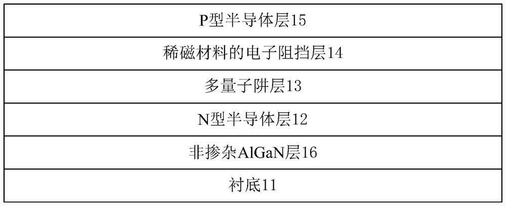
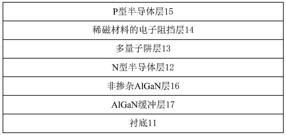
[0047] refer to figure 1 , figure 1 A schematic structural diagram of a deep ultraviolet LED provided by an embodiment of the present invention.

[0048] The deep ultraviolet LED comprises:

[0049] Substrate 1...


PUM

PropertyMeasurementUnit
thicknessaaaaaaaaaa
temperatureaaaaaaaaaa
thicknessaaaaaaaaaa

Abstract

The invention provides a deep ultraviolet LED and a manufacturing method thereof. The deep ultraviolet LED comprises a substrate; an N-type semiconductor layer, a multi-quantum well layer, an electron blocking layer and a P-type semiconductor layer which are sequentially arranged on one side of the substrate, wherein the electron blocking layer is made of diluted magnetic materials. The electron blocking layer of the diluted magnetic material can block electrons and also has a forward effect on hole injection, space wave function overlapping of the electrons and the holes is improved, and then the light emitting efficiency of the deep ultraviolet LED is improved.

Description

technical field [0001] The invention relates to the technical field of light-emitting diodes, and more specifically, to a deep ultraviolet LED and a manufacturing method thereof. Background technique [0002] With the continuous development of science and technology, various LED (Light Emitting Diode, light emitting diode) devices have been widely used in people's life and work, bringing great convenience to people's daily life. [0003] In recent years, AlGaN-based deep ultraviolet light-emitting diodes (UV-LEDs) have been widely used, for example, in the fields of air and water purification, surface disinfection, ultraviolet curing and medical phototherapy. [0004] According to the wavelength characteristics, the ultraviolet band can usually be divided into: long-wave ultraviolet UVA (wavelength range of 320nm-400nm), medium-wave ultraviolet UVB (wavelength range of 280nm-320nm), short-wave ultraviolet UVC (wavelength range of 200nm-280nm) and vacuum ultraviolet ( The wa...

Claims


Application Information

Patent Timeline
Patent Type & Authority Applications(China)
IPC IPC(8): H01L33/14H01L33/06H01L33/00
CPCH01L33/145H01L33/06H01L33/0075
Inventor 霍丽艳滕龙吴洪浩周瑜刘兆
Owner XIAMEN CHANGELIGHT CO LTD
Why Eureka
Try Eureka