Novel negative electrode current collector, negative electrode composed of novel negative electrode current collector and lithium ion battery
A lithium-ion battery and current collector technology, applied in the direction of electrode carrier/current collector, battery electrode, secondary battery, etc., to achieve high energy density, speed up coating efficiency, and alleviate the effect of fracture
- Summary
- Abstract
- Description
- Claims
- Application Information
AI Technical Summary
Problems solved by technology
Method used
Image
Examples
preparation example Construction
[0047] The preparation of the positive electrode sheet is as follows: the positive electrode slurry is coated on the current collector, where the current collector is preferably aluminum, and its thickness is 9-16 microns, and the thickness of the positive electrode slurry coated on the surface of the current collector is 0.3 Micron to 0.8 micron, coating weight from 0.4g / m2 to 1.5g / m2 2 . This current collector has the characteristics of light weight and good electrical conductivity, and has great advantages in the extension and tensile strength of the pole piece.
[0048] The composition of the positive electrode slurry is the mass ratio of positive electrode material: conductive agent: binder = 96:2.3:1.7. The positive electrode material is composed of a layered ternary material and a one-dimensional olivine structure lithium iron phosphate material, which can be a ternary single material NCM111, NCM622, NCM523, or one or two of iron lithium materials, LFP, LMFP, It can a...
Embodiment 1
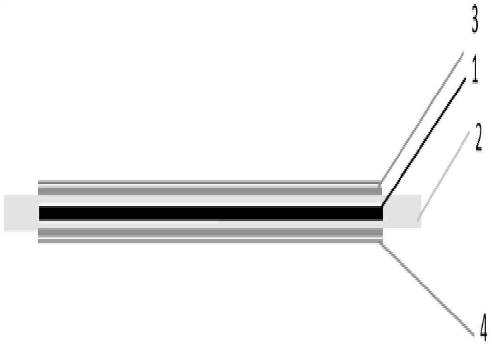
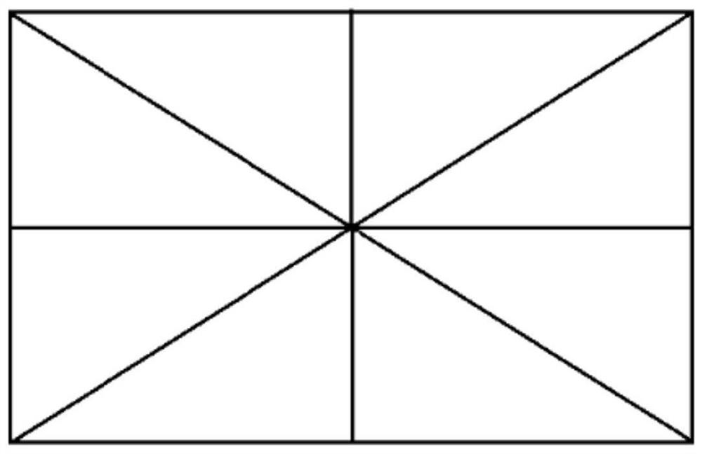
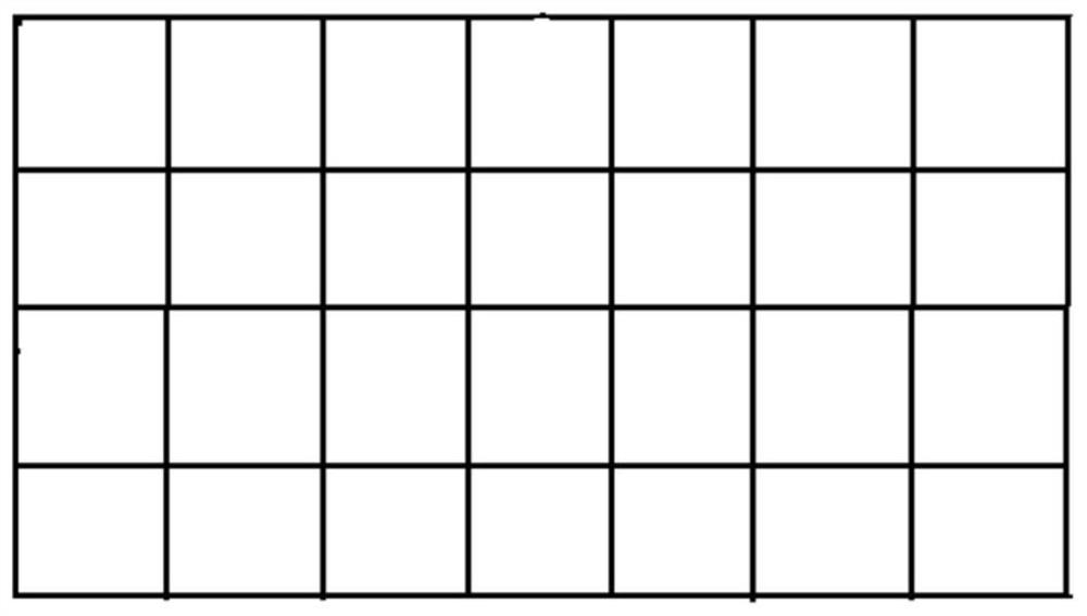
[0052] The surface density is 2g / m 2 , a melting point of 600° C., a thickness T0 of 2 μm, and a colorless and transparent base layer. And the base layer is grid-like. The conductive metal layer is prepared by a simple electroless plating method. The metal used is copper, which is peeled off to the base layer and left evenly. The thickness of the conductive metal layer is 6μm, and the surface density is 10g / m 2 , the sum of the surface density of it and the base layer is 12g / m 2 .
[0053] A porous conductive layer with a mass ratio of conductive agent to high molecular polymer of 8:2 is attached to the conductive metal layer, wherein the particle size of the conductive agent is between 1 nm, and it is uniformly distributed on the surface of the high molecular polymer. The polymer is polyvinylidene fluoride, and no additional solvent is needed in the process. A very thin composite binder layer is coated on the surface of the porous conductive layer, the main substance of t...
Embodiment 2
[0060] The surface density is 4g / m 2 , with a melting point of 1300° C. and a thickness T0 of 2 μm, is a colorless and transparent base layer, and the base layer is grid-like. The conductive metal layer is prepared by a simple electroless plating method. The metal used is copper, which is peeled off to the base layer and left evenly. The thickness of the conductive metal layer is 6μm, and the surface density is 10g / m 2 , the sum of the surface density of it and the base layer is 12g / m 2 .
[0061] A porous conductive layer with a mass ratio of conductive agent to high molecular polymer of 8:2 is attached to the conductive layer, wherein the particle size of the conductive agent is between 1nm, which is evenly distributed on the surface of the high molecular polymer, and the high molecular polymer is polymerized The material is polyvinylidene fluoride, and no additional solvent is added during the process. A very thin composite binder layer is coated on the surface of the po...
PUM
| Property | Measurement | Unit |
|---|---|---|
| electrical conductivity | aaaaa | aaaaa |
| tensile strength | aaaaa | aaaaa |
| thickness | aaaaa | aaaaa |
Abstract
Description
Claims
Application Information
 - R&D
- Intellectual Property
- Life Sciences
- Materials
- Tech Scout
- Unparalleled Data Quality
- Higher Quality Content
- 60% Fewer Hallucinations
Browse by: Latest US Patents, China's latest patents, Technical Efficacy Thesaurus, Application Domain, Technology Topic, Popular Technical Reports.
© 2025 PatSnap. All rights reserved.Legal|Privacy policy|Modern Slavery Act Transparency Statement|Sitemap|About US| Contact US: help@patsnap.com


