Check patentability & draft patents in minutes with Patsnap Eureka AI!

Preparation method of split-gate flash memory

A technology of memory and flash memory, which is applied in the field of preparation of split-gate flash memory, can solve problems such as programming crosstalk failure, and achieve the effect of improving device performance

Pending Publication Date: 2021-06-15
SHANGHAI HUAHONG GRACE SEMICON MFG CORP
View PDF0 Cites 0 Cited by
  • Summary
  • Abstract
  • Description
  • Claims
  • Application Information

AI Technical Summary

Problems solved by technology

[0005] The purpose of the present invention is to provide a preparation method of split-gate flash memory to solve the problem of programming crosstalk failure caused by leakage current

Method used


Image

  • Preparation method of split-gate flash memory
  • Preparation method of split-gate flash memory
  • Preparation method of split-gate flash memory

Examples


preparation example Construction

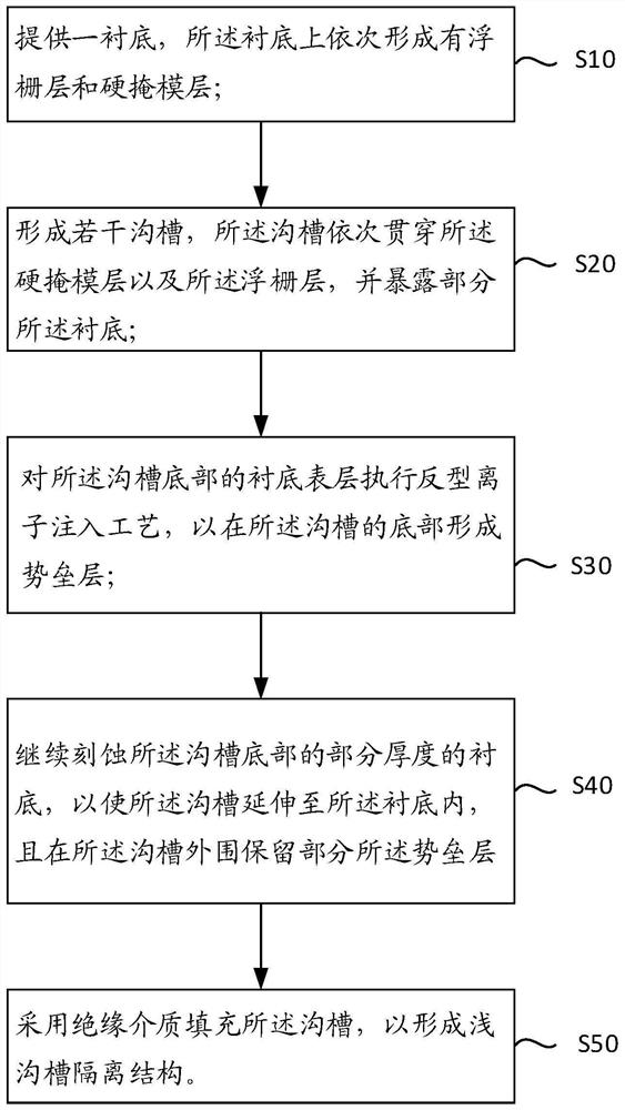
[0038] In order to solve the above technical problems, this embodiment provides a method for preparing a split-gate flash memory, please refer to 1, including:

[0039] Step 1 S10: providing a substrate, on which a floating gate layer and a hard mask layer are sequentially formed.

[0040] Step 2 S20 : ​​forming a plurality of trenches, the trenches sequentially penetrate through the hard mask layer and the floating gate layer, and expose part of the substrate.

[0041] Step 3 S30: performing an inverse ion implantation process on the substrate surface layer at the bottom of the trench to form a barrier layer at the bottom of the trench.

[0042] Step 4 S40 : continue to etch the bottom part of the thickness of the substrate, so that the trench extends into the substrate, and retain part of the barrier layer around the trench.

[0043] Step 5 S50: filling the trench with an insulating medium to form a shallow trench isolation structure.


PUM


Abstract

The invention provides a preparation method of a split-gate flash memory. The preparation method comprises the following steps that: a substrate on which a floating gate layer and a hard mask layer are sequentially formed is provided; a plurality of grooves are formed, the grooves sequentially penetrate through the hard mask layer and the floating gate layer, and part of the substrate is exposed. an inversion ion implantation process is performed on the surface layer of the substrate at the bottom of the grooves so as to form a barrier layer at the bottoms of the grooves; the substrate at the bottoms of the grooves is further etched by a part of thickness, so that the grooves extend into the substrate, and a part of the barrier layer at the peripheries of the grooves is reserved; the grooves are filled with an insulating medium to form shallow groove isolation structures. Therefore, the inversion ion implantation process is performed on the grooves before the grooves are filled, so that the barrier layer is formed at the bottoms of the grooves, leakage current is prevented from entering the device to cause programming crosstalk failure, and the performance of the device is improved.

Description

technical field [0001] The invention relates to the technical field of semiconductor manufacturing, in particular to a method for preparing a split-gate flash memory. Background technique [0002] Flash memory is a kind of non-volatile memory. Its operating principle is to control the switch of the gate channel by changing the critical voltage of the transistor or memory cell to achieve the purpose of storing data, so that the data stored in the memory will not be affected by the power supply. interrupted and disappeared. Now flash memory has occupied most of the market share of non-volatile semiconductor memory, becoming the fastest growing non-volatile semiconductor memory. Among them, according to the classification of the gate structure, the flash memory is mainly divided into a divided gate structure and a stacked gate structure. Compared with stacked-gate flash memory, split-gate flash memory has higher programming efficiency, and the word line structure can avoid "o...

Claims


Application Information

Patent Timeline
Patent Type & Authority Applications(China)
IPC IPC(8): H01L21/8246H01L21/336H01L21/762H01L21/265H10B20/00
CPCH01L29/66825H01L21/76237H01L21/76224H01L21/265
Inventor 汤志林王卉
Owner SHANGHAI HUAHONG GRACE SEMICON MFG CORP
Features
  • R&D
  • Intellectual Property
  • Life Sciences
  • Materials
  • Tech Scout
  • Unparalleled Data Quality
  • Higher Quality Content
  • 60% Fewer Hallucinations
Learn More