Patterned substrate, light -emitting diode and manufacturing method thereof

A technology for patterning substrates and manufacturing methods, which is applied to semiconductor devices, electrical components, circuits, etc., can solve the problems of difficult p-GaN layer and transparent electrode layer patterning procedures, etc., so as to improve light extraction efficiency and simple process method. , the effect of improving the internal quantum efficiency

Active Publication Date: 2021-06-18
FUJIAN JING AN OPTOELECTRONICS CO LTD
View PDF5 Cites 0 Cited by
  • Summary
  • Abstract
  • Description
  • Claims
  • Application Information

AI Technical Summary

Problems solved by technology

However, it is difficult to actually commercialize the patterning process of p-GaN layer and transparent electrode layer considering the formation of p-type electrode after patterning, the manufacturing process of light emitting diode (such as packaging process or the like) and the yield

Method used


Image

  • Patterned substrate, light -emitting diode and manufacturing method thereof
  • Patterned substrate, light -emitting diode and manufacturing method thereof
  • Patterned substrate, light -emitting diode and manufacturing method thereof

Examples


Embodiment 1

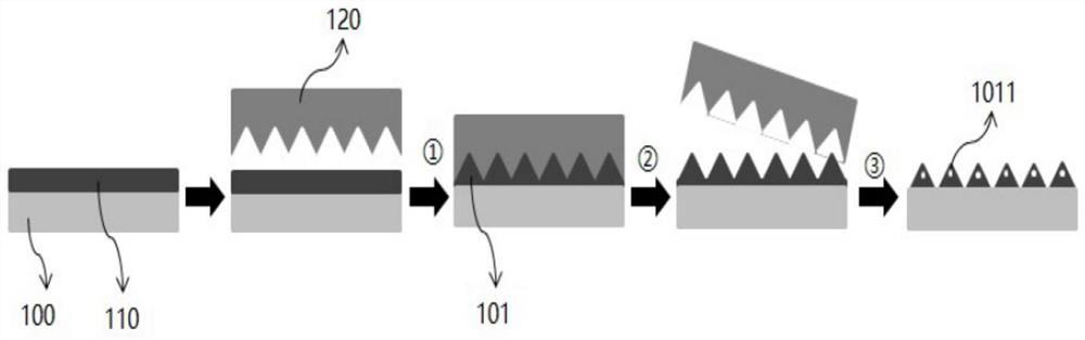
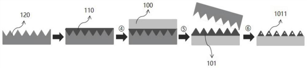
[0052] like figure 1 Shown is the processing method of the patterned substrate provided in this embodiment,

[0053] forming a convex structure on the surface of the substrate;

[0054] There are two methods for forming the convex structure. The convex forming method selected in this embodiment is as follows: figure 2 Imprinting method shown. like figure 2 As shown, a layer of solution is applied on the surface of the substrate 100 to form the coating 110; the nano-mold 120 is used to imprint the substrate, and the process ① shown in the figure is imprinting, and the substrate 100 and the nano-mold 120 are separated , the process ② shown in the figure is the stripping process, the substrate 100 and the convex structure 101 are subjected to the process ③ in the figure, that is, ultraviolet light treatment and annealing treatment to form a convex structure with pores 1011 inside.

[0055] The substrate surface coating solution can be selected from any of the following: SiO...

Embodiment 2

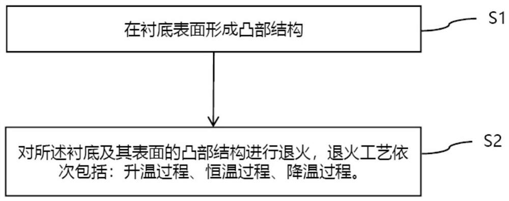
[0073] This embodiment discloses a light-emitting diode, which includes the patterned substrate described in Embodiment 1 and an epitaxial layer formed on the surface of the patterned substrate, wherein the epitaxial layer includes a convex structure formed on the patterned substrate in turn. A first semiconductor layer on one side, an active layer, and a second semiconductor layer of the opposite type to the first semiconductor layer. This embodiment also discloses a method for manufacturing a light-emitting diode: forming a convex structure on the surface of the substrate; annealing the substrate and the convex structure on the surface, and the annealing process sequentially includes: a heating process, a constant temperature process, and a cooling process; the Refer to Embodiment 1 for the fabrication method of the patterned substrate, which will not be repeated here. The manufacturing method of the light emitting diode in this embodiment further includes sequentially prepa...


PUM

PropertyMeasurementUnit
thicknessaaaaaaaaaa
refractive indexaaaaaaaaaa

Abstract

The invention provides a patterned substrate, a light-emitting diode and a manufacturing method of the patterned substrate, and the method comprises the following steps: forming a convex part structure on the surface of the substrate through the imprinting or reprinting of a nanometer mold, and carrying out the annealing treatment of the convex part structure on the surface of the substrate, and uniformly distributed pores are generated in the convex part structure by controlling parameters of an annealing process, so that the patterned substrate with high porosity inside is obtained. The patterned substrate, the light-emitting diode and the manufacturing method of the patterned substrate and the light-emitting diode are simple and economical, the light extraction efficiency can be remarkably improved through the manufactured patterned substrate and the manufactured light-emitting diode, and therefore the brightness of an LED is improved.

Description

technical field [0001] The invention relates to the technical field of semiconductor devices, in particular to a patterned substrate, a light-emitting diode and a preparation method thereof. Background technique [0002] Light-emitting diodes have attracted attention as a light source for future lighting, and have been widely used in many fields due to their long life, low energy consumption, and environmental friendliness compared to traditional fluorescent lamps, incandescent lamps and other light-emitting devices. light source. In particular, due to the large energy level difference of nitride light emitting diodes, it has the advantages of emitting green light to blue light region and near-ultraviolet light region, which greatly expands its application fields, such as LCD and mobile phone backlight, automotive lighting , traffic lights, general lighting, etc. However, there is no method that can effectively improve the performance of nitride light-emitting diodes. [...

Claims


Application Information

Patent Timeline
Patent Type & Authority Applications(China)
IPC IPC(8): H01L33/00H01L33/22H01L33/10
CPCH01L33/22H01L33/10H01L33/007
Inventor 李瑞评李彬彬彭鹏飞霍曜吴福仁梅晓阳
Owner FUJIAN JING AN OPTOELECTRONICS CO LTD
Why Eureka
Try Eureka