
3D semiconductor device and forming method thereof

A semiconductor and device technology, applied in the field of 3D semiconductor devices and their formation, can solve the problems of increasing static power consumption of MOS devices, reducing device reliability, and decreasing gate control capability of MOS devices, reducing short-channel effects, increasing Channel length, wafer area saving effect

Active Publication Date: 2021-06-22
晶芯成(北京)科技有限公司
View PDF6 Cites 3 Cited by
  • Summary
  • Abstract
  • Description
  • Claims
  • Application Information

AI Technical Summary

Problems solved by technology

However, when the size of the MOS device is reduced to a certain extent, the short channel effect will be caused
The short channel effect will lead to a decrease in the control ability of the gate of the MOS device, which will cause a shift in the threshold voltage and a drain-induced barrier lowering effect, resulting in an increase in the static power consumption of the MOS device
At the same time, the reduced device size will lead to an increase in the electric field inside the device, which will increase the generation of hot carriers and reduce the reliability of the device.

Method used


Image

  • 3D semiconductor device and forming method thereof
  • 3D semiconductor device and forming method thereof
  • 3D semiconductor device and forming method thereof

Examples


Embodiment Construction

[0050] As mentioned in the background, at present, in the manufacture of integrated circuit devices, in order to pursue high device performance and save the chip area occupied by each device, the size of MOS devices continues to shrink. However, as the MOS device continues to shrink, the channel length of the MOS device shrinks and the thickness of the tunnel oxide layer becomes thinner and thinner. However, when the size of the MOS device is reduced to a certain extent, the short channel effect will be induced. The short channel effect will lead to a decrease in the control ability of the gate of the MOS device, which will cause a threshold voltage drift and a drain-induced barrier lowering effect, resulting in an increase in the static power consumption of the MOS device. At the same time, the shrinking device size will lead to an increase in the electric field inside the device, increasing the generation of hot carriers and reducing the reliability of the device.

[0051] ...


PUM


Abstract

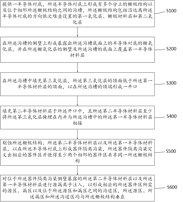
The invention provides a 3D semiconductor device and a forming method thereof, and is applied to the technical field of semiconductors. According to the forming method of the 3D semiconductor device provided by the invention, a grid electrode is shared by two adjacent MOS devices, the grid electrode and the drain electrode / source electrodes of the MOS devices are arranged on the surface of the semiconductor substrate, and the grid electrode and the drain electrode / source electrodes are horizontally connected, so that the width of the grid electrode of the MOS devices can be increased in the vertical direction, the 3D semiconductor device can be formed, and the channel length of the MOS device is increased, and the wafer area can be saved under the condition of reducing the short channel effect of the MOS device.

Description

technical field [0001] The invention relates to the technical field of semiconductors, in particular to a 3D semiconductor device and a forming method thereof. Background technique [0002] The scaling of features in integrated circuits has been the driving force behind the continued growth of the semiconductor industry over the past few decades. Scaling to smaller and smaller features enables increased densities of functional units on the limited chip area of ​​semiconductor chips. For example, shrinking transistor size allows combining increased numbers of memory or logic devices on a chip, resulting in products with increased capacity. However, the drive to greater and greater capacity is not without its problems. The need to optimize the performance of each device is becoming more and more important. [0003] At present, in the manufacture of integrated circuit devices, in order to pursue high performance of devices and save the chip area occupied by each device, the ...

Claims


Application Information

Patent Timeline
Patent Type & Authority Applications(China)
IPC IPC(8): H01L21/336H01L29/78H01L29/423
CPCH01L29/42356H01L29/66484H01L29/7831
Inventor 杨家诚汪文婷
Owner 晶芯成(北京)科技有限公司
Learn More