System and method for machining nanoelectrode on material substrate through femtosecond laser

A femtosecond laser and nano-electrode technology, applied in the field of femtosecond laser applications, can solve problems affecting the performance of micro-electrodes, short-circuit faults, etc., and achieve the effects of reducing the risk of short-circuit faults, high positioning accuracy, and high motion accuracy

Active Publication Date: 2021-07-02
TSINGHUA UNIV +1
View PDF5 Cites 0 Cited by
  • Summary
  • Abstract
  • Description
  • Claims
  • Application Information

AI Technical Summary

Problems solved by technology

Due to the conductivity of the processed two-dimensional material, the material debris accumulated in the ablation tank will affect the performance of the microelectrode, which m

Method used


Image

  • System and method for machining nanoelectrode on material substrate through femtosecond laser
  • System and method for machining nanoelectrode on material substrate through femtosecond laser
  • System and method for machining nanoelectrode on material substrate through femtosecond laser

Examples


Embodiment 1

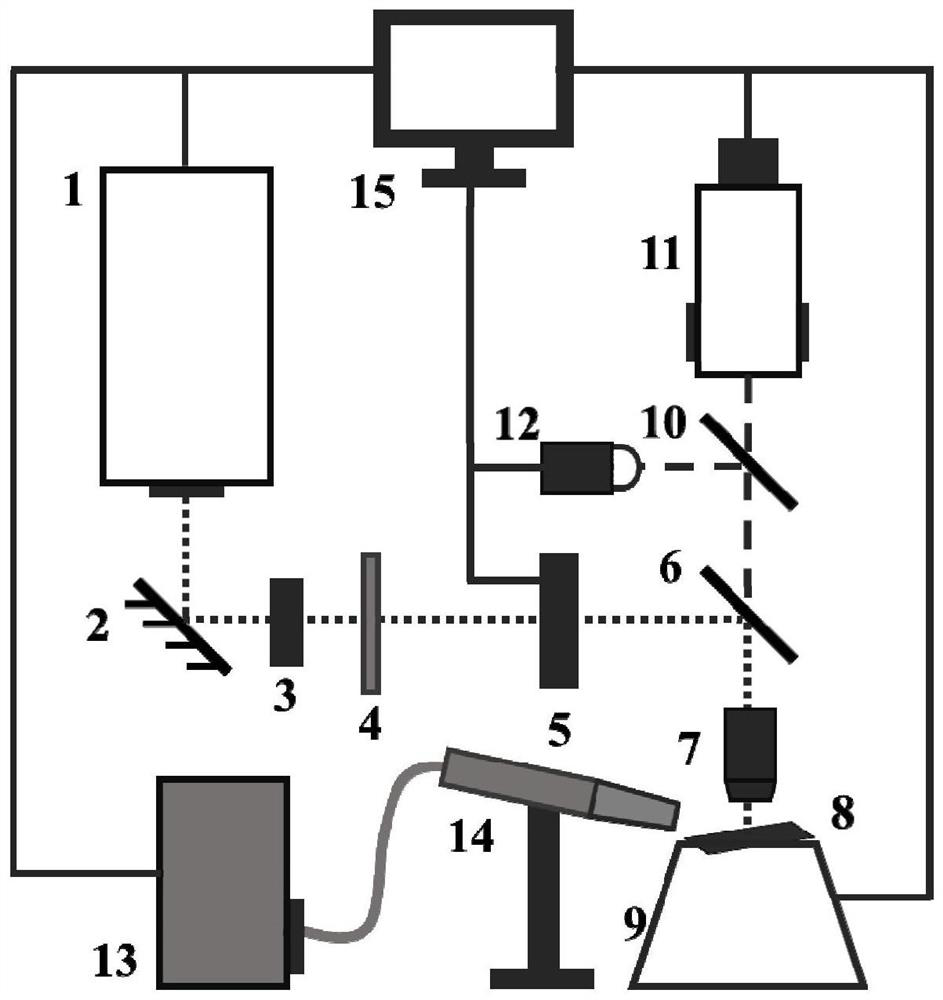
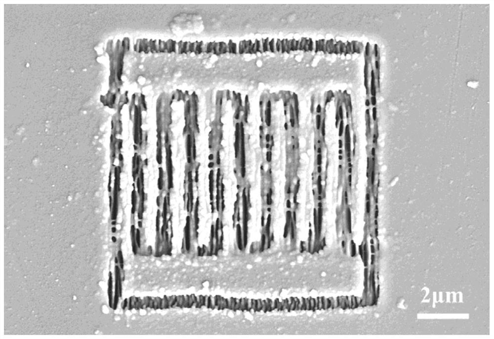
[0028] Fabrication of nanometer interdigitated electrodes on two-dimensional material substrates using femtosecond laser. Turn on the femtosecond laser 1, adjust the aperture 2 so that the spot diameter is 4 mm, adjust the position of the telephoto high-power objective lens 7 so that the focus falls near the surface of the high-precision three-dimensional motion platform 9, close the electronically controlled shutter 5, turn on the CCD 11 and the lighting lamp 12, Adjust the height of the high-precision three-dimensional motion platform 9 and the CCD 11 to make the image clear, adjust the attenuation plate 4 to make the power of the femtosecond laser 5-10 μW, adjust the height of the high-precision three-dimensional motion platform 9 to focus the femtosecond laser on the two-dimensional material sample 8 , turn on the air pump 13, align the blowing port 14 with the two-dimensional material sample 8, adjust the air pressure of the air pump 13 to 20 kPa, so that a uniform and sta...

Embodiment 2

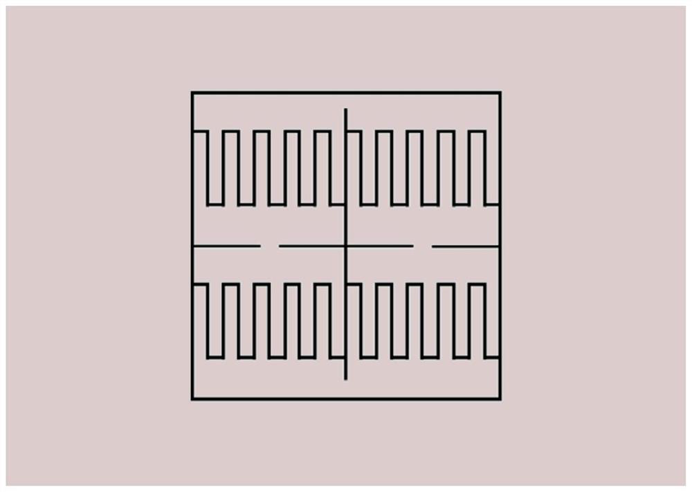
[0031] A 2×2 series-parallel array of interdigitated electrodes is processed on a two-dimensional material substrate by using a femtosecond laser. Turn on the femtosecond laser 1, adjust the aperture 2 so that the spot diameter is 4 mm, adjust the position of the telephoto high-power objective lens 7 so that the focus falls near the surface of the high-precision three-dimensional motion platform 9, close the electronically controlled shutter 5, turn on the CCD 11 and the lighting lamp 12, Adjust the height of the high-precision three-dimensional motion platform 9 and the CCD 11 to make the image clear, adjust the attenuation plate 4 to make the power of the femtosecond laser 5-10 μW, adjust the height of the high-precision three-dimensional motion platform 9 to focus the femtosecond laser on the two-dimensional material sample 8 , turn on the air pump 13, align the blowing port 14 with the two-dimensional material sample 8, adjust the air pressure of the air pump 13 to 20 kPa, ...


PUM

PropertyMeasurementUnit
Diameteraaaaaaaaaa

Abstract

The invention belongs to the technical field of femtosecond laser application, and particularly relates to a system and method for machining a nanoelectrode on a material substrate through femtosecond laser. The system comprises key parts such as a long-focus high-power objective lens, a high-precision three-dimensional motion platform and an air blowing system. The long-focus high-power objective lens focuses a laser spot to a submicron level, so that the machining line width reaches a hundred-nanometer level, thereby realizing the machining of the nanoelectrode, the high-precision three-dimensional motion platform is high in positioning precision, the straightness of line scanning meets the machining requirement in the machining of a nanometer scale, the blowing system can remove material scraps generated in the machining process, and accumulation of material scraps is reduced. According to the method, femtosecond laser direct writing machining is used to ablate and remove the materials in a scanning area to realize the machining of the nanoelectrode on the two-dimensional material substrate. The system and method of the present invention can flexibly, quickly and accurately machine a variety of nanoelectrodes and nanoelectrode arrays on the two-dimensional material substrate.

Description

technical field [0001] The invention belongs to the field of femtosecond laser application technology, and in particular relates to a system and method for processing nanometer electrodes on a material matrix by using femtosecond laser. Background technique [0002] The characteristic size of the microelectrode is micron or smaller. With different electrolytes, it can be used in supercapacitors, sensors and other devices. The micro-interdigitated electrode is composed of two interdigitated finger electrodes. Microelectrodes are conducive to improving the integration of circuit systems, and can also be used to manufacture micro components, which have important applications in chemical, biological, environmental and other fields. The factors affecting the performance of microelectrodes include the distance between electrodes and the area of ​​electrodes. Microelectrodes are called nanoelectrodes when the characteristic scale reaches the nanometer level, and the reduction of t...

Claims


Application Information

Patent Timeline
IPC IPC(8): B23K26/046B23K26/142B23K26/36
CPCB23K26/142B23K26/046B23K26/36
Inventor 姜澜闫剑锋郭恒黄辰潇
Owner TSINGHUA UNIV
Why Eureka
Try Eureka