High-performance silicon carbide semiconductor field effect transistor structure

A field-effect transistor and high-performance silicon carbide technology, which is applied in the field of high-performance silicon carbide semiconductor field-effect transistor structure, can solve the problems of unfixed wiring, inconvenient maintenance, and low electrode hardness, and achieve simple and convenient opening and closing, and easy maintenance , Reasonable effect of assembly

Active Publication Date: 2021-07-02
陈甲锋
View PDF7 Cites 1 Cited by
  • Summary
  • Abstract
  • Description
  • Claims
  • Application Information

AI Technical Summary

Problems solved by technology

[0004] 1. The electrode hardness of the existing high-performance silicon carbide semiconductor field effect transistor structure is low, and it is easy to bend or break the electrode during use, resulting in damage to the high-performance silicon carbide semiconductor field effect transistor;
[0005] 2. During the use of the existing high-performance silicon carbide semiconductor field effect transistor structure, when a fault occurs inside the high-performance silicon carbide semiconductor field effect transistor structure, maintenance is inconvenient;
[0006] 3. The internal wiring of the existing high-performance silicon carbide semiconductor field effect transistor structure is not fixed, and the unreasonable wiring will cause the wires to be intertwined and entangled together, which is likely to cause damage to the structure of the high-performance silicon carbide semiconductor field effect transistor

Method used


Image

  • High-performance silicon carbide semiconductor field effect transistor structure
  • High-performance silicon carbide semiconductor field effect transistor structure
  • High-performance silicon carbide semiconductor field effect transistor structure

Examples


Embodiment 1

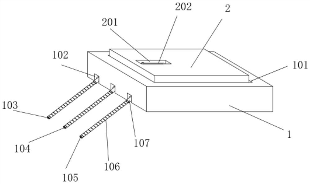
[0035] see Figure 1-2, in an embodiment of the present invention, a high-performance silicon carbide semiconductor field effect transistor structure includes a field effect transistor body, the field effect transistor body includes a field effect transistor base 1 and a field effect transistor outer cavity 2, and the field effect transistor The outer cavity 2 is fastened on the top surface of the field effect transistor base 1, and several groups of wiring frames 3 are arranged between the field effect transistor base 1 and the field effect transistor outer cavity 2. One side of the field effect transistor base 1 Three rotating slots 102 are provided, and the insides of the three rotating slots 102 are respectively provided with a hinge shaft 108, and a T-shaped connecting frame 107 is rotatably connected to the hinge shaft 108, and one side of the field effect transistor base 1 A transistor collector 103, a transistor base 104, and a transistor emitter 105 are respectively p...

Embodiment 2

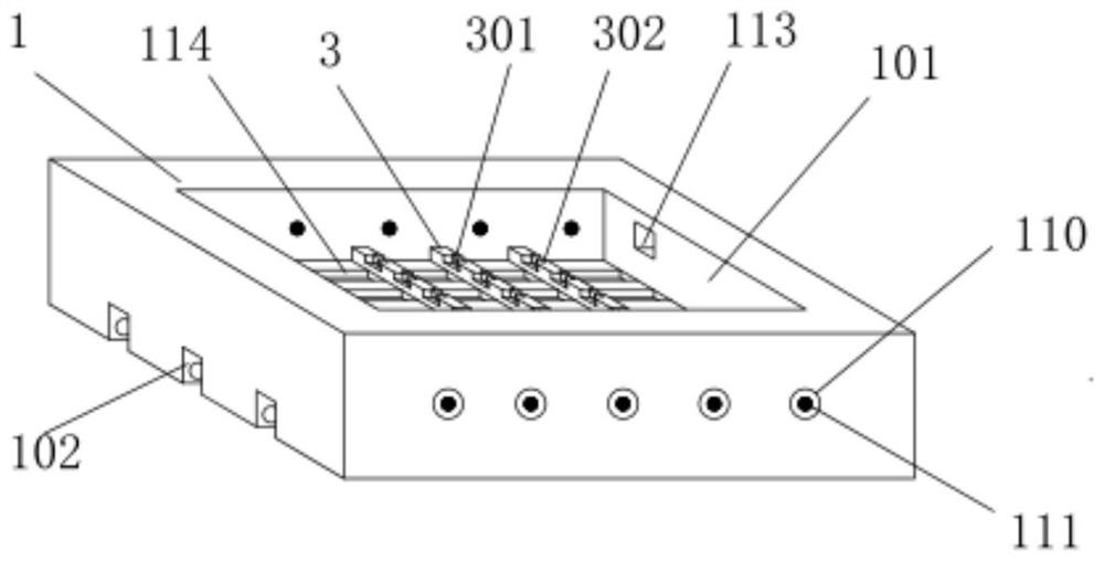
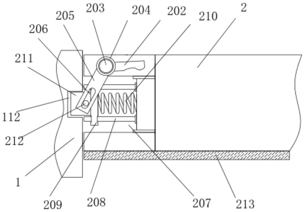
[0038] see image 3 , this embodiment is basically the same as Embodiment 1. Preferably, the top surface of the field effect transistor base 1 is provided with an inner groove 101 for erecting the outer cavity 2 of the field effect transistor, and the inner wall on the left side of the inner groove 101 The middle position of the inner groove 101 is provided with a card slot 112, and the two ends of the inner wall on the right side of the inner groove 101 are provided with a fixing groove 113, and the left end surface of the field effect transistor outer cavity 2 and the inner groove 101 is provided with a concave The hollow groove 207, the upper and lower sides of the hollow groove 207 are horizontally provided with guide rods 208, the guide rod 208 is slidably connected with a guide block 209, and the right end surface of the guide block 209 is provided with a spring 210, so The other end of the spring 210 is in contact with the inner wall of the hollow groove 207, and the le...

Embodiment 3

[0042] see figure 2 , this embodiment is basically the same as Embodiment 1. Preferably, the wiring frame 3 includes several wiring boards arranged in the inner groove 101 of the field effect transistor base 1, and the inner bottom surface of the inner groove 101 is provided with Several strip-shaped slots 114, the wiring board is clamped in the strip-shaped slot 114 through the limit block on the bottom surface, and several wiring slots 301 are equidistantly opened on the wiring board, and the wiring slots 301 Positioning holes 302 are opened on both sides of the cable trough 301, and a limit bar 303 is arranged above the cable trough 301. The two ends of the bottom surface of the limit bar 303 are provided with positioning rubber heads 304 that are compatible with the positioning holes 302. The position bar 303 is clamped in the positioning hole 302 by the positioning rubber head 304. The left end of the wiring groove 301 has a trumpet-shaped projected area in the vertical ...


PUM


Abstract

A high-performance silicon carbide semiconductor field effect transistor structure disclosed by the present invention comprises a field effect transistor body, the field effect transistor body comprises a field effect transistor base and a field effect transistor outer cavity, and the field effect transistor outer cavity is internally buckled on the top surface of the field effect transistor base. A plurality of groups of cabling racks are arranged between the field effect transistor base and the field effect transistor outer cavity, three rotating grooves are formed in one side of the field effect transistor base, first hinged shafts are arranged in the three rotating grooves respectively, and T-shaped connecting frames are rotationally connected to the first hinged shafts. The wiring board is provided with the wiring groove, and the wiring groove is arranged to be of a horn-shaped structure with a large left end opening and a small right end opening, so the wiring groove can achieve the integrated installation of a plurality of wires, enables the internal structure assembly of the field effect transistor body to be more reasonable, reduces the fault rate of the field effect transistor base body, and the service life of the field effect transistor base body is prolonged.

Description

technical field [0001] The invention belongs to the technical field of electronic components, in particular to a high-performance silicon carbide semiconductor field effect transistor structure. Background technique [0002] A transistor is a solid semiconductor device that can be used for detection, rectification, amplification, switching, voltage stabilization, signal modulation, and many other functions. The transistor acts as a variable switch that controls the outgoing current based on the input voltage. Therefore, transistors can be used as current switches. The difference from general mechanical switches (such as relay and switch) is that transistors are controlled by electrical signals, and the switching speed can be very fast. The switching speed in the laboratory can reach more than 100GHz. Strictly speaking, transistors generally refer to all single components based on semiconductor materials, including diodes, triodes, field effect transistors, thyristors, etc. m...

Claims


Application Information

Patent Timeline
Patent Type & Authority Applications(China)
IPC IPC(8): H01L23/053H01L23/16H01L23/10H01L23/367
CPCH01L23/053H01L23/10H01L23/16H01L23/3672
Inventor 陈甲锋
Owner 陈甲锋
Why Eureka
Try Eureka