Method for detecting quality of dielectric layer of micro-fluidic chip

A quality inspection method and microfluidic chip technology, applied in chemical instruments and methods, laboratory utensils, laboratory containers, etc., can solve problems such as process instability, foreign matter, and insufficient compactness.

Active Publication Date: 2021-07-06
AUTOBIO LABTEC INSTR CO LTD
View PDF6 Cites 0 Cited by
  • Summary
  • Abstract
  • Description
  • Claims
  • Application Information

AI Technical Summary

Problems solved by technology

The instability of the process can easily cause defects such as pinholes, foreign matter, unevenness, and insufficient compactness in the dielectric

Method used


Image

  • Method for detecting quality of dielectric layer of micro-fluidic chip
  • Method for detecting quality of dielectric layer of micro-fluidic chip
  • Method for detecting quality of dielectric layer of micro-fluidic chip

Examples


Embodiment Construction

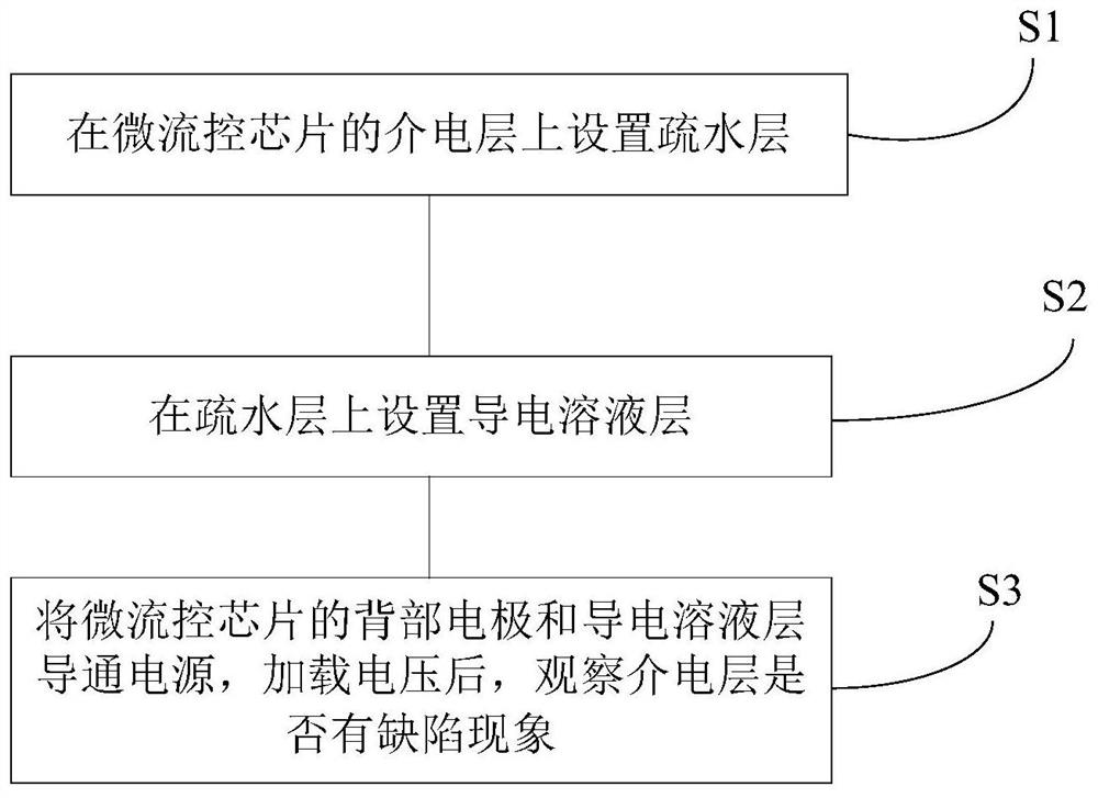
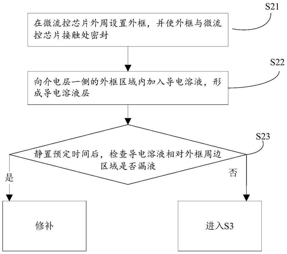
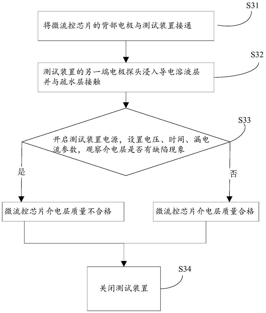
[0062] The following will clearly and completely describe the technical solutions in the embodiments of the present invention with reference to the accompanying drawings in the embodiments of the present invention. Obviously, the described embodiments are only some, not all, embodiments of the present invention. Based on the embodiments of the present invention, all other embodiments obtained by persons of ordinary skill in the art without making creative efforts belong to the protection scope of the present invention.

[0063] Please refer to the attached figure 1 And attached Figure 5 , figure 1 A schematic flow chart of the steps of a specific implementation of the method for detecting the quality of the dielectric layer of the microfluidic chip provided by the embodiment of the present invention, attached Figure 5 It is a schematic diagram of the detection structure of the dielectric layer of the microfluidic chip in the present invention.

[0064] In a specific embo...


PUM

PropertyMeasurementUnit
Depthaaaaaaaaaa

Abstract

The invention discloses a method for detecting the quality of a dielectric layer of a micro-fluidic chip. The method comprises the following steps: S1, arranging a hydrophobic layer on the dielectric layer of the micro-fluidic chip; s2, arranging a conductive solution layer on the hydrophobic layer; and s3, conducting a power supply on the back electrode of the micro-fluidic chip and the conductive solution layer, and observing whether the dielectric layer has a defect phenomenon or not after loading voltage; wherein the defect phenomenon comprises at least one of bubble generation and color change of the conductive solution layer, electric spark generation of the dielectric layer and leakage current sudden increase; the hydrophobic layer is arranged on the dielectric layer, the conductive solution layer is arranged on the hydrophobic layer for electrifying detection of the to-be-tested electrode area, it is indicated that the dielectric layer has defects as long as at least one of bubble generation, color change, electric spark generation and leakage current sudden increase of the conductive solution layer occur in the testing process, and the method is easy to operate and high in detection efficiency; and large-area detection can be carried out.

Description

technical field [0001] The invention relates to the technical field of microfluidic chips, in particular to a method for detecting a defect in a dielectric layer of a microfluidic chip. Background technique [0002] Existing microfluidic chip dielectric layer defect detection mainly includes breakdown voltage method and optical microscope detection method: [0003] The former is to plate a certain thickness of dielectric layer on the conductive area of ​​the microfluidic chip to be protected by physical or chemical methods. According to the thickness of the dielectric material, the breakdown voltage of the dielectric material is estimated, and then the two ends of the chip are (One end is the conductive area, the other end is the dielectric area) respectively connected to the positive and negative poles of the power supply, input the estimated voltage, after a period of time, if there is a defect in the dielectric layer at this position, leakage breakdown will occur, through...

Claims


Application Information

Patent Timeline
IPC IPC(8): B01L3/00
CPCB01L3/5027B01L2200/143
Inventor 杨柳青刘永强张东锋赵克丽郝茂垒李超王超刘聪
Owner AUTOBIO LABTEC INSTR CO LTD
Why Eureka
Try Eureka