
Etching solution, touch panel and manufacturing method of touch panel

A technology of a touch panel and a manufacturing method, which is applied in the direction of instruments, electrical digital data processing, and input/output process of data processing, etc., and can solve the problem of inability to meet the narrow frame requirements of the display, the inability to reduce the size of the lead wires in the peripheral area, and the size enlargement, etc. question

Pending Publication Date: 2021-07-16
CAMBRIOS FILM SOLUTIONS CORP
View PDF5 Cites 1 Cited by
  • Summary
  • Abstract
  • Description
  • Claims
  • Application Information

AI Technical Summary

Problems solved by technology

[0003] However, there are still many problems to be solved in the nanowire manufacturing technology, such as using nanowires to make touch electrodes, and the alignment error area needs to be reserved when the nanowires and the leads in the peripheral area are aligned. The bit error area causes the size of the lead wires in the peripheral area to be unable to be reduced, which in turn leads to a larger width in the peripheral area, especially in the roll-to-roll (Roll to Roll) process, and the deformation of the substrate causes the size of the alignment error area to be further enlarged (eg 150um), so that the minimum width of the peripheral area is only 2.5mm, so it cannot meet the narrow border requirements of the display
Furthermore, the choice of etching solution is also a problem

Method used


Image

  • Etching solution, touch panel and manufacturing method of touch panel
  • Etching solution, touch panel and manufacturing method of touch panel
  • Etching solution, touch panel and manufacturing method of touch panel

Examples


Embodiment Construction

[0081] A number of embodiments of the present invention will be disclosed below with the accompanying drawings. For the sake of clarity, many practical details will be described together in the following description. It should be understood, however, that these practical details should not be used to limit the invention. That is, in some embodiments of the present invention, these practical details are unnecessary. In addition, for the sake of simplification of the drawings, some conventional structures and components are simply shown in the drawings.

[0082] As used herein, "about", "approximately" or "approximately" generally means that the error or range of the value is within 20%, preferably within 10%, more preferably within Within five percent. If there is no explicit statement in the text, the numerical values ​​mentioned are all regarded as approximate values, that is, there are errors or ranges indicated by "about", "approximately" or "approximately".

[0083] The...


PUM

PropertyMeasurementUnit
thicknessaaaaaaaaaa
thicknessaaaaaaaaaa
thicknessaaaaaaaaaa

Abstract

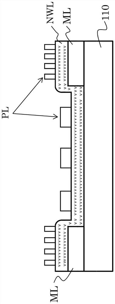
The invention discloses an etching solution, a touch panel and a manufacturing method of the touch panel, and the manufacturing method of the touch panel comprises the following steps: providing a substrate which is provided with a display region and a peripheral region; a metal layer and a metal nanowire layer are arranged, the first part of the metal nanowire layer is located in the display region, and the second part of the metal nanowire layer and the metal layer are located in the peripheral region; the patterning step comprises the steps that etching liquid capable of etching the metal layer and the metal nanowire layer is used for forming a plurality of peripheral leads on the metal layer and forming a plurality of etching layers on the second part of the metal layer at the same time, and the etching liquid comprises hydrogen peroxide (0.2-40 wt%), acid (0.2-20 wt%), a metal corrosion inhibitor (0.1-10 wt%) and / or a stabilizing agent (0.1-10 wt%). In addition, the invention also provides an etching solution and a touch panel. Patterning of the metal nanowire layer or the metal layer is directly carried out through the etching liquid, so that the purpose of simplifying the manufacturing process is achieved, and the manufacturing cost is further controlled.

Description

technical field [0001] The invention relates to an etchant, a touch panel and a manufacturing method thereof. Background technique [0002] In recent years, transparent conductors can simultaneously allow light to pass through and provide proper conductivity, and thus are often used in many display or touch-related devices. Generally speaking, the transparent conductor can be various metal oxides, such as indium tin oxide (Indium Tin Oxide, ITO), indium zinc oxide (Indium Zinc Oxide, IZO), cadmium tin oxide (Cadmium Tin Oxide, CTO) or aluminum-doped oxide Zinc (Aluminum-doped Zinc Oxide, AZO). However, these metal oxide thin films cannot meet the flexibility requirements of display devices. Therefore, a variety of flexible transparent conductors have been developed, for example, transparent conductors made of materials such as nanowires. [0003] However, there are still many problems to be solved in the nanowire manufacturing technology, such as using nanowires to make t...

Claims


Application Information

Patent Timeline
Patent Type & Authority Applications(China)
IPC IPC(8): G06F3/044
CPCG06F3/0445G06F3/0446G06F2203/04103
Inventor 萧仲钦练修成萧啓帆蔡家扬邱逸文
Owner CAMBRIOS FILM SOLUTIONS CORP
Learn More