

Packaging structure and packaging method thereof, and display device
A technology of packaging structure and packaging method, which is applied in the manufacturing of electrical components, electric solid-state devices, semiconductor/solid-state devices, etc., can solve the problems of inability to simultaneously isolate water and oxygen erosion and evacuate the heat of devices, and avoid poor thermal conductivity, poor performance and poor performance. Structural stability and anti-erosion effect
- Summary
- Abstract
- Description
- Claims
- Application Information
AI Technical Summary
Problems solved by technology
Method used
Image

Examples
Embodiment 1
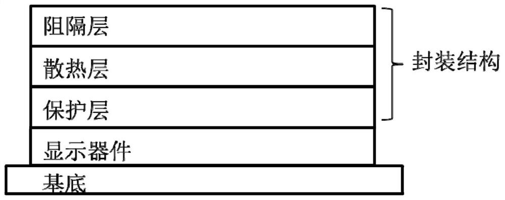
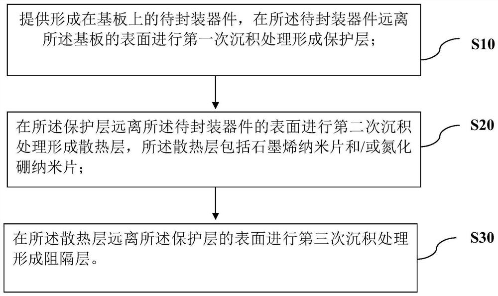
[0062] A display device, comprising the steps of:
[0063] ① providing a device to be packaged formed on the substrate, depositing an aluminum nitride film layer on the surface of the device to be packaged away from the substrate to form a protective layer with a thickness of 100 to 500 nanometers;
[0064] ② Depositing graphene nanosheets with a height of 10 to 50 nanometers on the surface of the protective layer away from the device to be packaged, so that the graphene nanosheets are arranged perpendicular to the protective layer, forming a density of 50 to 300 pieces / micron 2 heat dissipation layer;
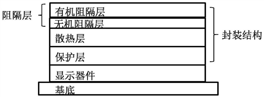
[0065] ③ Deposit Al first on the surface of the heat dissipation layer away from the protective layer 2 o 3 film layer, forming a first inorganic barrier layer with a thickness of 100 to 200 nanometers, and then depositing polyethylene terephthalate on the surface of the first inorganic barrier layer to form an organic barrier layer with a thickness of 200 to 400 nanometers ...
Embodiment 2
[0067] A display device, comprising the steps of:
[0068] ① Provide a substrate containing the same device to be packaged as in Example 1, and deposit an aluminum nitride film layer on the surface of the device to be packaged away from the substrate to form a protective layer with a thickness of 100 to 500 nanometers;
[0069]② Depositing boron nitride nanosheets with a height of 10 to 50 nanometers on the surface of the protective layer away from the device to be packaged, so that the boron nitride nanosheets are arranged perpendicular to the protective layer, and the formation density is 50 to 300 / Micron 2 heat dissipation layer;
[0070] ③ Deposit Al first on the surface of the heat dissipation layer away from the protective layer 2 o 3 film layer, forming a first inorganic barrier layer with a thickness of 100 to 200 nanometers, and then depositing polyethylene terephthalate on the surface of the first inorganic barrier layer to form an organic barrier layer with a t...
Embodiment 3
[0072] A display device, comprising the steps of:
[0073] ① Provide a substrate containing the same device to be packaged as in Example 1, and deposit an aluminum nitride film layer on the surface of the device to be packaged away from the substrate to form a protective layer with a thickness of 100 to 500 nanometers;
[0074] ② Depositing graphene nanosheets and boron nitride nanosheets with a height of 10 to 50 nanometers on the surface of the protective layer away from the device to be packaged, so that the graphene nanosheets and boron nitride nanosheets are perpendicular to the protective layer Set, forming a density of 50 to 300 / micron 2 heat dissipation layer;
[0075] ③ Deposit Al first on the surface of the heat dissipation layer away from the protective layer 2 o 3 film layer, forming a first inorganic barrier layer with a thickness of 100 to 200 nanometers, and then depositing polyethylene terephthalate on the surface of the first inorganic barrier layer to fo...
PUM
| Property | Measurement | Unit |
|---|---|---|
| Thickness | aaaaa | aaaaa |
| Thickness | aaaaa | aaaaa |
| Thickness | aaaaa | aaaaa |
Abstract
Description
Claims
Application Information