Multi-microelectrode integrated sensing chip and application in biochemical enzyme-free rapid detection
A sensor chip and microelectrode technology, applied in the field of electrochemical detection, can solve the problems of electrochemical sensors that are difficult to reuse, enzymes that are sensitive to the external environment, and easy to deactivate
- Summary
- Abstract
- Description
- Claims
- Application Information
AI Technical Summary
Problems solved by technology
Method used
Image
Examples
Embodiment 1
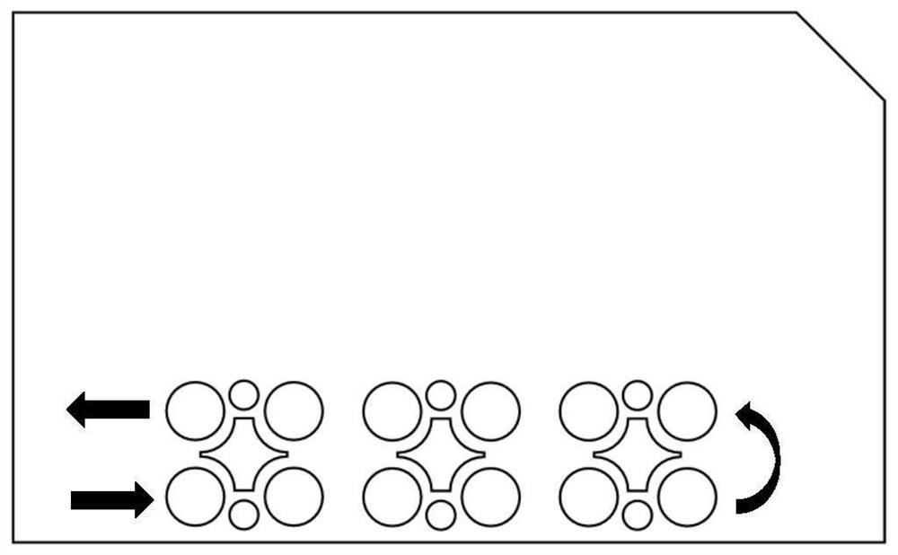
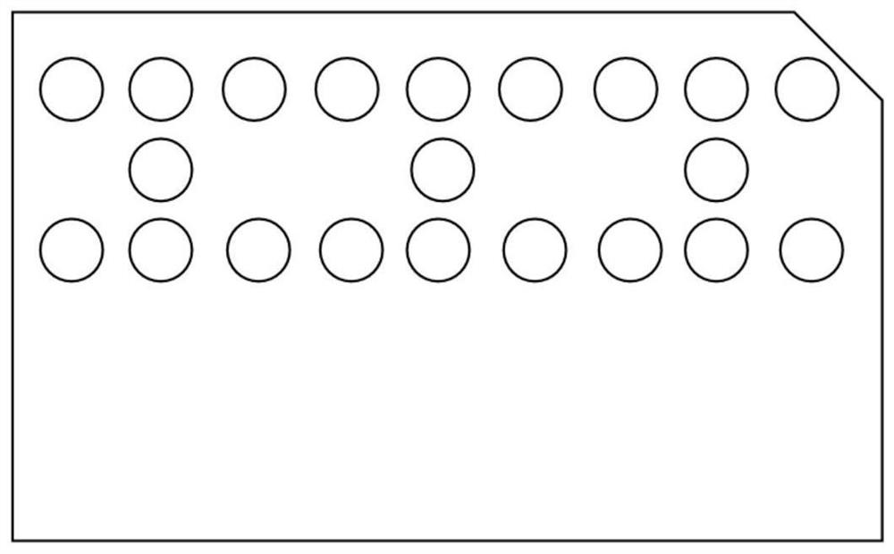
[0068] A detection area is set on the front of the microelectrode integrated sensor chip, and multiple microelectrode modules are set in the detection area. Specific electrodes, wherein the distance between the working electrode and the counter electrode in the microelectrode module is 0.20-0.25 mm, and the distance between the working electrodes is 1.0-1.5 mm. The working electrode includes an electrode layer and a modified layer, wherein the electrode layer includes an electrode base Cu layer and a conductive inner layer of Ni layer from bottom to top, the thickness of the Cu layer is 10.0-15.0 μm, and the thickness of the Ni layer is 2.0-5.0 μm.
[0069] Modify the nanoporous copper modification layer on the surface of the working electrode, specifically electroplating copper-tin alloy on the surface of the microelectrode, with a current density of 5A / dm 2 , electrodeposited at a temperature of 35°C for 550s, and then put it into a 10% sulfuric acid solution for dealloying ...
Embodiment 2
[0071] A detection area is set on the front of the microelectrode integrated sensor chip, and multiple microelectrode modules are set in the detection area. Specific electrodes, wherein the distance between the working electrode and the counter electrode in the microelectrode module is 0.20-0.25 mm, and the distance between the working electrodes is 1.0-1.5 mm. The working electrode includes an electrode layer and a modified layer, wherein the electrode layer includes an electrode base Cu layer and a conductive inner layer of Ni layer from bottom to top, the thickness of the Cu layer is 10.0-15.0 μm, and the thickness of the Ni layer is 2.0-5.0 μm.
[0072] Modify the nanoporous gold modification layer on the surface of the working electrode, specifically, electroplate gold-tin alloy on the surface of the microelectrode for 5 minutes, and then place it in a 2M NaOH+1M NaCl mixed solution for dealloying treatment, using platinum as the counter electrode, and the voltage Set to ...
Embodiment 3
[0074] A detection area is set on the front of the microelectrode integrated sensor chip, and multiple microelectrode modules are set in the detection area. Specific electrodes, wherein the distance between the working electrode and the counter electrode in the microelectrode module is 0.20-0.25 mm, and the distance between the working electrodes is 1.0-1.5 mm. The working electrode includes an electrode layer and a modification layer, wherein the electrode layer includes an electrode substrate Cu layer, a conductive inner layer of Ni layer and a reaction layer Au layer from bottom to top. The thickness of the Cu layer is 10.0-15.0 μm, and the thickness of the Ni layer is 2.0 ~5.0μm, the Au layer thickness is 0.05~0.10μm.
[0075]Modify the nanoporous silver modification layer on the surface of the working electrode, specifically, electroplate silver-tin alloy on the surface of the microelectrode, keep stirring at room temperature for 5 minutes, and then put it into 4M KOH+1M ...
PUM
| Property | Measurement | Unit |
|---|---|---|
| thickness | aaaaa | aaaaa |
| thickness | aaaaa | aaaaa |
| thickness | aaaaa | aaaaa |
Abstract
Description
Claims
Application Information


