

Semiconductor device
A semiconductor and device technology, applied in the field of semiconductor devices, can solve the problems of reduced electrostatic discharge protection ability and high cost
- Summary
- Abstract
- Description
- Claims
- Application Information
AI Technical Summary
Problems solved by technology
Method used
Image

Examples
Embodiment 1
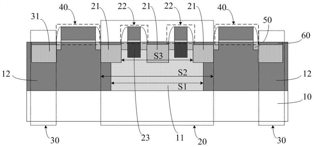
[0027] figure 1 This is a schematic structural diagram of the semiconductor device provided in this embodiment. This embodiment provides a semiconductor device to improve the ESD capability of the device and reduce the manufacturing cost of the device. Please refer to figure 1 , the semiconductor device includes a substrate 10 , three sub-drain regions 21 , two dummy structures 22 , a source region 31 and a gate structure 40 .
[0028] The substrate 10 has a first area 20 and a second area 30 , and the first area 20 is located between two adjacent second areas 30 . The substrate 10 has the second conductivity type, and the material of the substrate 10 includes one or more of silicon, germanium, gallium, nitrogen or carbon. Both the first well region 11 and the second well region 12 are located in the substrate 10 , the first well region 11 is located between two adjacent second well regions 12 , wherein the first well region 11 In the first region 20 of the substrate 10 , ...
Embodiment 2
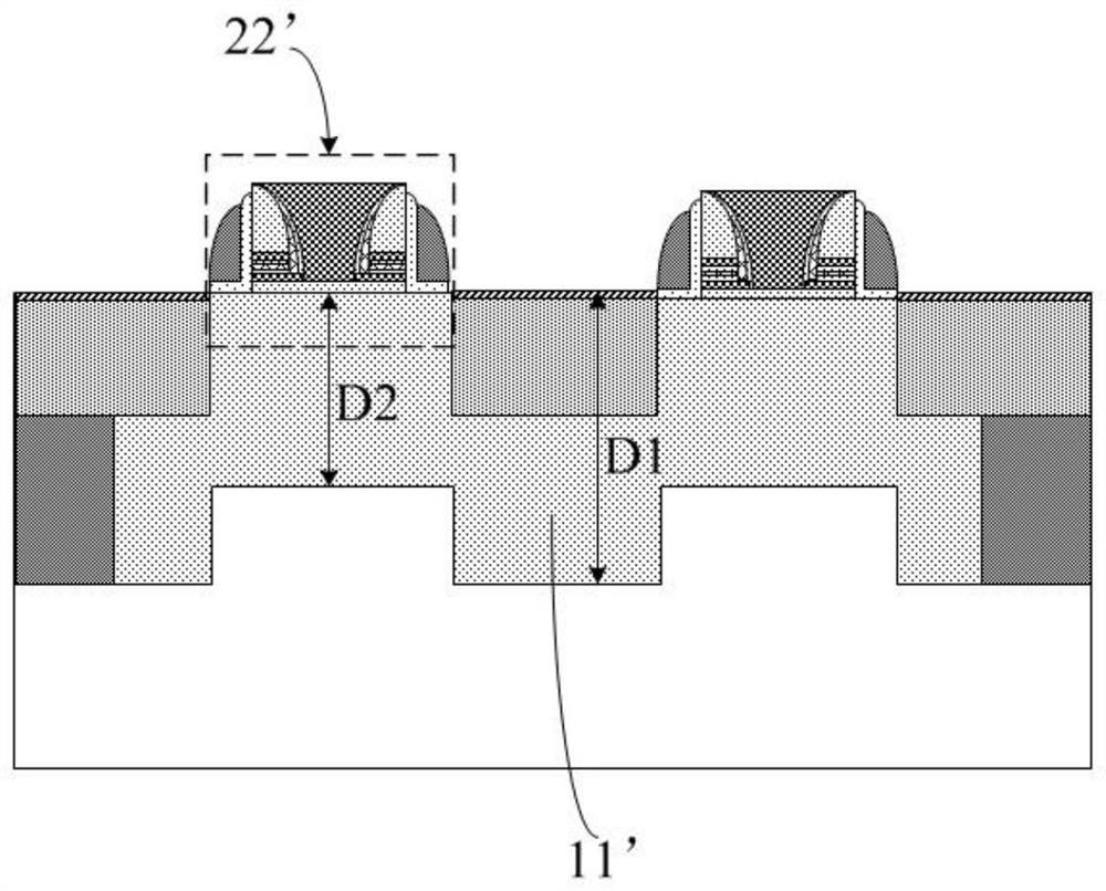
[0036] figure 2 This is a partial structural schematic diagram of the semiconductor device provided in this embodiment. Please refer to figure 2 , figure 2 Provided for Example 1 figure 1 Schematic diagram of the structure at the first area, the difference between this embodiment and Embodiment 1 is that the structure of the dummy structure 22' is different. In this embodiment, the dummy structure 22' is a FLASH structure. The structure will not be described in detail, and those skilled in the art can configure it according to the actual situation. In this embodiment, neither the SAB mask of the prior art nor the introduction of a new process flow is required. The dummy structure 22' is simultaneously fabricated in the FLASH structure preparation process, and no redundant mask is required, and no new process is required. Process flow, reducing the mask can save the manufacturing cost of the device.
[0037] In this embodiment, it is not necessary to form a shallow tren...
PUM
 Abstract
Description
Claims
Application Information