Dual-beam cavity-backed antenna based on artificial electromagnetic structure and cavity odd-mode excitation
A dual-beam, odd-mode technology, applied in the field of dual-beam cavity-backed antennas, can solve the problems of reducing antenna profile, radiation asymmetry, narrow bandwidth, etc., and achieve the effect of simple feeding structure, good radiation performance, and beam width compression.
- Summary
- Abstract
- Description
- Claims
- Application Information
AI Technical Summary
Problems solved by technology
Method used
Image
Examples
Embodiment 1
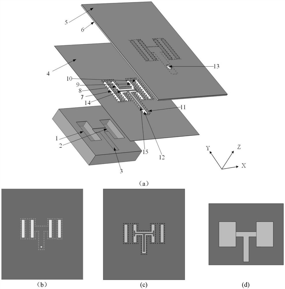
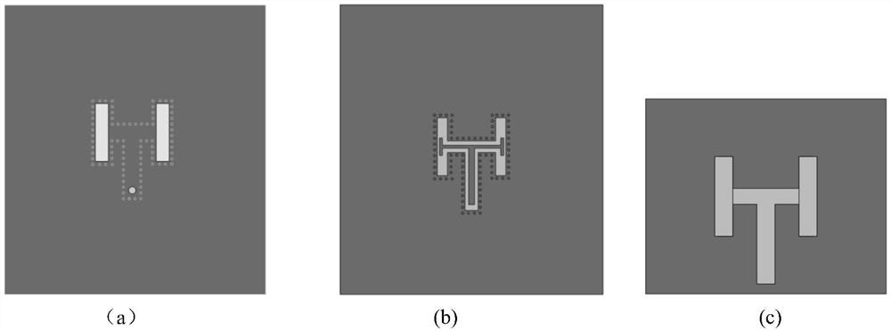
[0042] This embodiment provides an ultra-wideband, low sidelobe, dual-beam cavity-backed antenna based on cavity odd-mode excitation, and its overall structure schematic diagram is as follows figure 1 As shown in (a), it includes a metal block, a lower metal layer 4, a dielectric substrate 6 and an upper metal layer 5; the lower metal layer is located on the upper surface of the metal block and on the lower surface of the dielectric substrate; the upper metal layer is located on the upper surface of the dielectric substrate Surface; the centers of the metal block, lower metal layer, dielectric substrate and upper metal layer coincide; the side lengths of the lower metal layer, upper metal layer and dielectric substrate are the same (90mm×100mm), and are longer than the side length of the metal block.
[0043] The schematic diagram of the structure of the metal block is shown in figure 1 As shown in (d), two mirror-symmetrical rectangular back cavities 1 and 2 with a depth of 5...
Embodiment 2
[0057] This embodiment provides a broadband, low sidelobe, high gain, dual-beam cavity-backed antenna based on artificial electromagnetic structure and cavity odd-mode excitation technology. Based on the antenna described in Embodiment 1, the thickness of the dielectric substrate is modified It is 1.5mm, and it is used as the primary radiation source, and a transmissive metasurface composed of 9×9 metasurface elements is loaded directly above the antenna to compress the beam width and increase the far-field gain of the antenna.
[0058] The dielectric substrate 6 is made of Arlon IsoClad 917, with a relative permittivity of 2.17, a loss tangent of 0.0013, and a thickness of 1.5mm.
[0059] The top view of the transmissive metasurface is shown as Figure 4 As shown in (b), it consists of 9×9 metasurface units. The transmissive metasurface is placed directly above the antenna, and its lower surface is separated from the upper metal layer 5 by 20 mm.
[0060] The schematic diag...
PUM
 Abstract
Description
Claims
Application Information


