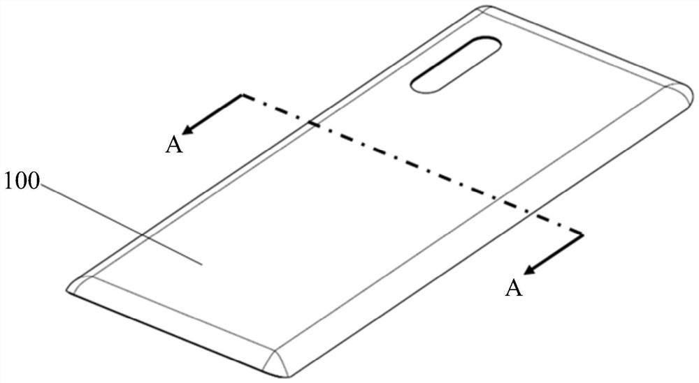
Shell assembly, manufacturing method thereof and electronic equipment
A shell assembly and manufacturing method technology, which is applied in the direction of electrical equipment shells/cabinets/drawers, chemical instruments and methods, shells/cabinets/drawer parts, etc., and can solve problems such as high cost and heavy shell weight
- Summary
- Abstract
- Description
- Claims
- Application Information
AI Technical Summary
Problems solved by technology
Method used
Image
Examples
Embodiment 1
[0078] This embodiment provides a shell assembly and a manufacturing method thereof. The housing assembly of this embodiment includes a ceramic base, an adhesion promoter layer, and a fiber-reinforced resin layer. The fiber-reinforced resin layer is connected to the ceramic base through an adhesion promoter layer. The thickness of the ceramic substrate is 0.6mm, the thickness of the adhesion promoter layer is 22μm, and the thickness of the fiber reinforced resin layer is 0.32mm.
[0079] The manufacturing method of the housing assembly of the present embodiment includes the following steps:
[0080] The zirconia ceramic base material is subjected to numerical control machining, cutting and grinding, and is thinned to a sheet shape with a thickness of 0.3 mm to obtain a ceramic base.
[0081] Clean the thinned ceramic substrate. The polyurethane adhesion promoter is evenly coated on the non-appearance surface of the ceramic substrate to form an adhesion promoter layer.
[0...
Embodiment 2
[0089] This embodiment provides a shell assembly and a manufacturing method thereof. The housing assembly of this embodiment includes a ceramic base, an adhesion promoter layer, and a fiber-reinforced resin layer. The fiber-reinforced resin layer is connected to the ceramic base through an adhesion promoter layer. The thickness of the ceramic substrate is 0.7mm, the thickness of the adhesion promoter layer is 22μm, and the thickness of the fiber reinforced resin layer is 0.3mm.
[0090] The manufacturing method of the housing assembly of the present embodiment includes the following steps:
[0091] The zirconia ceramic base material is subjected to numerical control machining, cutting and grinding, and is thinned to a sheet shape with a thickness of 0.3 mm to obtain a ceramic base.
[0092] Clean the thinned ceramic substrate. The polyurethane adhesion promoter is evenly coated on the non-appearance surface of the ceramic substrate to form an adhesion promoter layer.
[00...
Embodiment 3
[0100] This embodiment provides a mobile phone, including the casing component, the display component and the circuit board provided by the first embodiment.
[0101] An installation space is defined between the display component and the casing component connected between the display component and the casing component. The circuit board is arranged in the installation space and electrically connected with the display component.
PUM
| Property | Measurement | Unit |
|---|---|---|
| Thickness | aaaaa | aaaaa |
| Thickness | aaaaa | aaaaa |
| Thickness | aaaaa | aaaaa |
Abstract
Description
Claims
Application Information
 - R&D
- Intellectual Property
- Life Sciences
- Materials
- Tech Scout
- Unparalleled Data Quality
- Higher Quality Content
- 60% Fewer Hallucinations
Browse by: Latest US Patents, China's latest patents, Technical Efficacy Thesaurus, Application Domain, Technology Topic, Popular Technical Reports.
© 2025 PatSnap. All rights reserved.Legal|Privacy policy|Modern Slavery Act Transparency Statement|Sitemap|About US| Contact US: help@patsnap.com


