Diode chip and manufacturing method thereof

A manufacturing method and diode technology, applied in the field of diodes, can solve problems such as poor heat dissipation capability, and achieve the effects of short reverse recovery time, improved heat dissipation capability, and low energy consumption

Inactive Publication Date: 2021-08-17
CHINA ZHENHUA GRP YONGGUANG ELECTRONICS CO LTD STATE OWNED NO 873 FACTORY
View PDF7 Cites 0 Cited by
  • Summary
  • Abstract
  • Description
  • Claims
  • Application Information

AI Technical Summary

Problems solved by technology

This diode is not suitable for the axial high-reliability package commonly used in current diodes, and the heat dissipation capability is relatively poor

Method used


Image

  • Diode chip and manufacturing method thereof
  • Diode chip and manufacturing method thereof
  • Diode chip and manufacturing method thereof

Examples


Embodiment Construction

[0039] The technical solution of the present invention is further described below, but the scope of protection is not limited to the description.

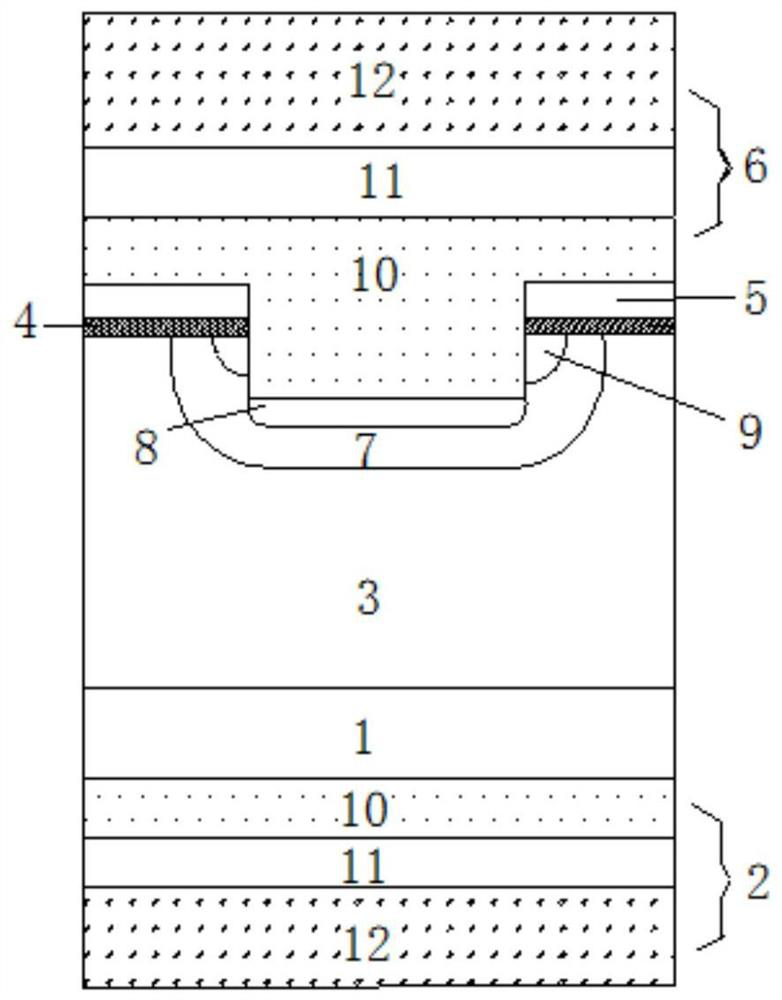
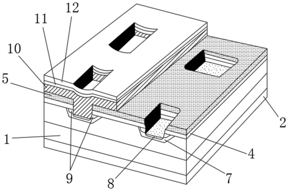
[0040] like Figure 1~2 Shown is the structural representation of cellular structure and diode chip of the present invention:

[0041] The invention provides a diode chip, which includes a plurality of cells connected in parallel with each other, the cells include an N+ substrate 1, a back metal layer 2 is provided on the back side of the N+ substrate 1, and a N+ substrate 1 is provided on the front side. - epitaxial region 3, the front of N-epitaxial region 3 is provided with gate oxide layer 4, polysilicon 5, metallization layer 6 in sequence; the front middle part of said N-epitaxial region 3 is embedded with P-type base region 7, metallization layer 6 There is a raised part on the back, and the raised part is embedded in the P-type base area 7, and the N+ area 9 is arranged around the raised part, and the P+ area 8 is arranged...


PUM

PropertyMeasurementUnit
thicknessaaaaaaaaaa
thicknessaaaaaaaaaa

Abstract

The invention provides a diode chip and a manufacturing method thereof. The chip comprises a plurality of cells which are connected in parallel, each cell comprises an N+ substrate, the back surface of each N+ substrate is provided with a back metal layer, the front surface of each N+ substrate is provided with an N- epitaxial region, and the front surface of each N- epitaxial region is sequentially provided with a gate oxide layer, polycrystalline silicon and a metallization layer; a P-type base region is embedded in the middle of the front face of the N- epitaxial region, a protruding part is arranged on the back face of the metallization layer, the protruding part is embedded into the P-type base region, an N+ region is arranged around the protruding part, a P+ region is arranged between the end face of the protruding part and the P-type base region, and the front faces of the P-type base region and the N+ region are covered with gate oxide layers. Compared with a PN junction structure, the device has the advantages of lower break-over voltage, shorter reverse recovery time and the like; compared with a Schottky diode, the Schottky diode has the advantages of good high-temperature characteristic, small electric leakage, positive temperature coefficient and the like; the conduction pressure drop is small, the energy consumption is low, the heat yield is small, and the durability is high; and a multi-cell parallel structure is adopted, so that the heat dissipation capability is greatly improved.

Description

technical field [0001] The invention relates to the technical field of diodes, in particular to a diode chip and a manufacturing method thereof. Background technique [0002] With the development of semiconductor technology, new structure diodes such as JBS, MPS, and TMPS have emerged in recent years, and the performance of diodes has also been continuously improved. However, the above structures are basically extended based on the traditional PN junction or Schottky junction structure, and cannot completely avoid the large forward voltage drop of the PN junction structure, the large reverse recovery time, and the high temperature of the Schottky junction structure. Poor characteristics, poor reliability and other issues. [0003] The Chinese patent with the publication number CN102709317A discloses a low turn-on voltage diode. The diode includes an N+ substrate, a metallized cathode on the back of the N+ substrate, and an N- epitaxial layer on the front. The surface of the...

Claims


Application Information

Patent Timeline
Patent Type & Authority Applications(China)
IPC IPC(8): H01L29/861H01L29/06H01L21/336H01L23/367
CPCH01L29/861H01L29/0603H01L29/0684H01L29/0692H01L29/6609H01L23/367
Inventor 袁强古进王博贺晓金陆超姚秋原
Owner CHINA ZHENHUA GRP YONGGUANG ELECTRONICS CO LTD STATE OWNED NO 873 FACTORY
Why Eureka
Try Eureka