Supercharge Your Innovation With Domain-Expert AI Agents!

Method for improving performance of front illumination type image sensor and front illumination type image sensor

An image sensor and front-illumination technology, applied in the field of image sensors, can solve the problems of sacrificing photon quantum efficiency, increasing sensitivity, and increasing the proportion of large-angle light

Pending Publication Date: 2021-08-31
GALAXYCORE SHANGHAI
View PDF0 Cites 0 Cited by
  • Summary
  • Abstract
  • Description
  • Claims
  • Application Information

AI Technical Summary

Problems solved by technology

The light is transmitted to the semiconductor metal interconnection layer 150 through the microlens 100 through the light-transmitting layer 120, and the light-absorbing layers 110 and 130 in several regions can be optionally designed during the optical path transmission; when the light is transmitted to the semiconductor metal interconnection layer 150, due to the previous The illuminated image sensor has several layers of metal layers (shown as M3 layer 140, M2 layer 141, and M1 layer 142 in the prior art), and the light will be diffracted at the opening of the optical path structure, and the diffracted light will reach adjacent pixels and cause Crosstalk, sacrificing photon quantum efficiency and reducing resolution accuracy
In addition, non-corresponding light with a large angle will also enter the current photoelectric conversion element, resulting in serious aliasing, which in turn affects the resolution accuracy
[0011] In the existing design, in order to reduce the influence of large angles, it is necessary to reduce the aperture size of the optical path structure, but the smaller the aperture size leads to the reduction of incident light and the enhancement of diffraction, which makes the photon quantum efficiency of the target photoelectric conversion element drop sharply, and finally the image signal becomes weaker. effect; and the opening becomes smaller, the sensitivity of the luminous flux that can enter the photoelectric conversion element in the optical system increases with the process fluctuation (lens size, shape, thickness of each layer, size of the opening, and alignment of each layer), which is not conducive to the realization of the device Batch stability of performance
[0012] In order to reduce the impact of light diffraction and large-angle light on the nearby photoelectric conversion elements, the solution of the existing technology needs to increase the buffer photoelectric conversion unit, which will lead to a larger chip area, which runs counter to market orientation and product demand.
[0013] Increasing the aperture size will increase the signal strength, but the proportion of large-angle light (not corresponding to the current photoelectric conversion element) will increase significantly, the anti-aliasing effect will deteriorate, the signal-to-noise ratio will deteriorate, and image clarity will be affected

Method used


Image

  • Method for improving performance of front illumination type image sensor and front illumination type image sensor
  • Method for improving performance of front illumination type image sensor and front illumination type image sensor
  • Method for improving performance of front illumination type image sensor and front illumination type image sensor

Examples


Embodiment Construction

[0042] In the following description, numerous specific details are set forth in order to provide a thorough understanding of the present invention. However, the present invention can be implemented in many other ways different from those described here, and those skilled in the art can make similar extensions without violating the connotation of the present invention, so the present invention is not limited by the specific implementations disclosed below.

[0043] Secondly, the present invention is described in detail by means of schematic diagrams. When describing the embodiments of the present invention in detail, for convenience of explanation, the schematic diagrams are only examples, which should not limit the protection scope of the present invention.

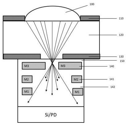
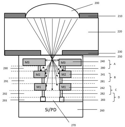
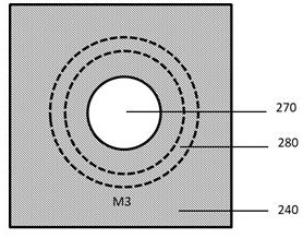
[0044] Please refer to figure 2 , figure 2It is a structural schematic diagram of the first embodiment of the front-illuminated image sensor involved in the present invention. Wherein, the light passes through the mic...


PUM


Abstract

The invention discloses a method for improving the performance of a front illumination type image sensor. An annular optical path at least with contact hole layer metal is formed in a light path structure of the front illumination type image sensor, the combination design of the hole opening size of the light path structure is conducted through the limitation of a plurality of metal layers, a contact hole layer and a polycrystalline silicon layer in the light path structure, crosstalk, caused by light divergence, of adjacent photosensitive units is eliminated or reduced, the design tolerance of the opening size of the light path structure is improved, and better sensitivity is achieved.

Description

technical field [0001] The invention relates to the field of image sensors, in particular to a method for improving the performance of a front-illuminated image sensor and the front-illuminated image sensor. Background technique [0002] An image sensor is a semiconductor device that converts light signals into electrical signals. The image sensor has a photoelectric conversion element. Usually, the photoelectric conversion element is formed under the substrate surface, and the logic circuit is formed on the photoelectric conversion element. After passing through the logic circuit, the light Before reaching the photoelectric conversion element, the light passes through the multi-layer structure, resulting in light loss or light crosstalk (crosstalk) to adjacent photoelectric conversion elements, affecting the photoresponse characteristics of each photoelectric conversion element. [0003] The current fingerprint identification schemes include optical technology, silicon tech...

Claims


Application Information

Patent Timeline
Patent Type & Authority Applications(China)
IPC IPC(8): H01L27/146
CPCH01L27/14625H01L27/14629H01L27/14623H01L27/14636
Inventor 郑展徐涛
Owner GALAXYCORE SHANGHAI
Features
  • R&D
  • Intellectual Property
  • Life Sciences
  • Materials
  • Tech Scout
  • Unparalleled Data Quality
  • Higher Quality Content
  • 60% Fewer Hallucinations
Learn More