Passivation contact structure and preparation method and application thereof
A contact structure, passivation layer technology, applied in the field of solar cells, can solve the problems of reducing cell efficiency, tunnel oxide layer damage, passivation performance degradation, etc., to achieve good integrity, reduce band gap, and prevent passivation. Effect
- Summary
- Abstract
- Description
- Claims
- Application Information
AI Technical Summary
Problems solved by technology
Method used
Image
Examples
Embodiment 1
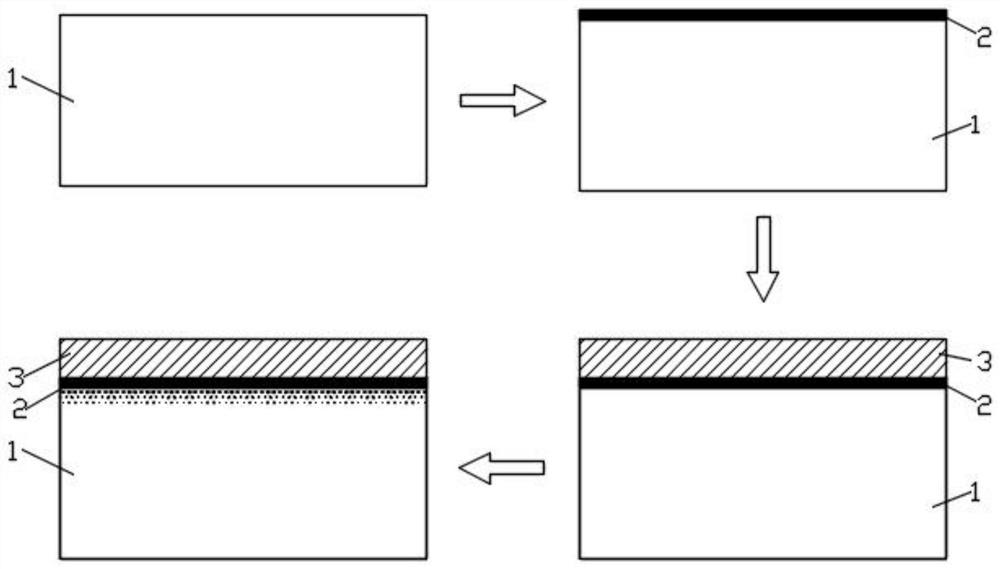
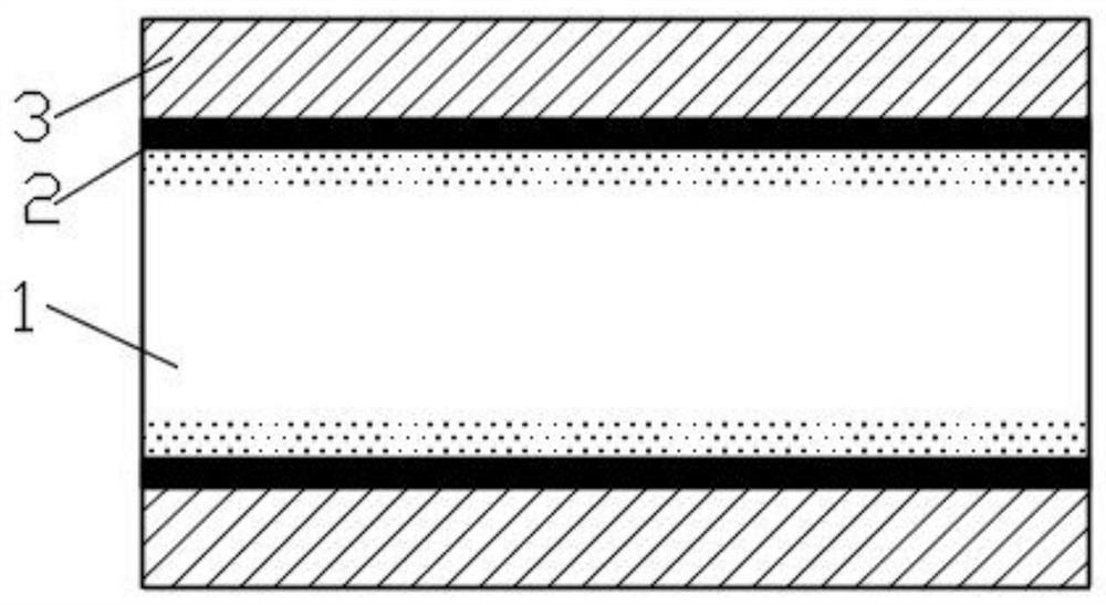
[0048] This embodiment provides a passivation contact structure, which includes a substrate 1 , a silicon oxycarbide passivation layer 2 and a doped polysilicon layer 3 are sequentially integrated on one surface of the substrate 1 .
[0049] Specifically, in this embodiment, the substrate 1 is an n-type crystalline silicon substrate 1 , and the doped polysilicon layer 3 is doped with phosphorus.
[0050] Further, the thickness of the silicon oxycarbide passivation layer 2 is 0.5-5nm, the doped oxygen atom content in the silicon oxycarbide passivation layer 2 is 5at%-50at%, and the doped carbon atom content is 0.1at%-20at% .
[0051] Specifically, the doped carbon atom content in the silicon oxycarbide passivation layer 2 is 0.1 at%, 1 at%, 5 at%, 10 at% or 20 at%, and in this embodiment, the doped carbon atom content is 10 at%.
[0052] Specifically, in order to effectively collect carriers, the silicon oxycarbide passivation layer 2 has a thickness of 1-3 nm, and the heavily...
Embodiment 2
[0061] Such as figure 1 As shown, this embodiment discloses a method for preparing a passivation contact structure, which is used to prepare the passivation contact structure in Embodiment 1. The preparation method includes sequentially preparing a silicon oxycarbide passivation layer 2 and a doped polysilicon precursor on one surface of a substrate 1 , and then performing high-temperature annealing and crystallization, and the doped polysilicon precursor forms a doped polysilicon layer 3 .
[0062] Further, the annealing temperature range is 800-1100°C.
[0063] Specifically, preparing the silicon oxycarbide passivation layer 2 and the doped polysilicon precursor sequentially on one surface of the substrate 1 refers to first preparing a layer of silicon oxycarbide passivation layer 2 on one surface of the substrate 1, and then A layer of doped polysilicon precursor is prepared on the surface of the silicon oxycarbide passivation layer 2 .
[0064] Further, the high-temperat...
Embodiment 3
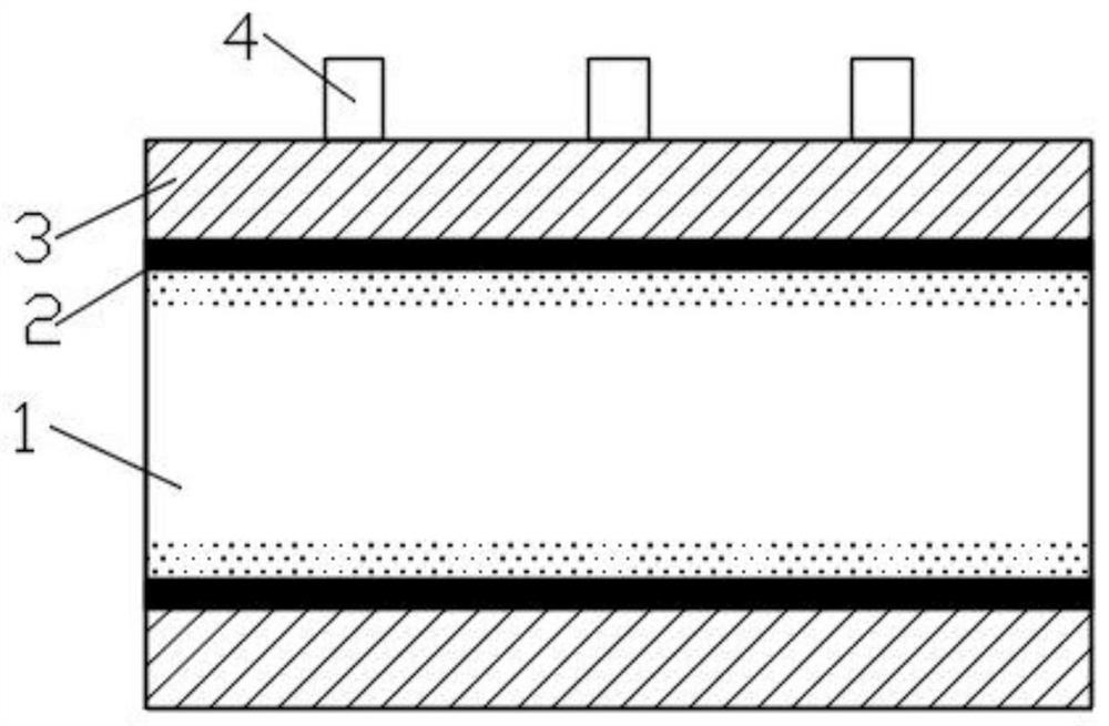
[0073] This embodiment provides an application of a passivation contact structure, and the passivation contact structure in Embodiment 1 is applied to a solar cell.
[0074] Specifically, the electrode 4 is prepared on the surface of the doped polysilicon layer 3 . In another embodiment, a polysilicon layer is prepared on the surface of the doped polysilicon layer 3 first, and then a layer of electrodes 4 is prepared on the surface of the polysilicon layer.
PUM
| Property | Measurement | Unit |
|---|---|---|
| thickness | aaaaa | aaaaa |
| thickness | aaaaa | aaaaa |
| thickness | aaaaa | aaaaa |
Abstract
Description
Claims
Application Information


