Copper-based thick-wall Nb3Sn thin film superconducting cavity and preparation method thereof

A superconducting cavity, thin film technology, applied in the field of superconductivity, can solve problems such as failure

Active Publication Date: 2021-09-10
INST OF MODERN PHYSICS CHINESE ACADEMY OF SCI
View PDF17 Cites 1 Cited by
  • Summary
  • Abstract
  • Description
  • Claims
  • Application Information

AI Technical Summary

Problems solved by technology

However, high-quality Nb 3 The formation of Sn requires a high temperature environment higher than 930 °C
Therefore, limited by the low melting point of oxygen-free copper, in the world by directly growing high-quality Nb on the inner surface of the oxygen-free copper substrate cavity 3 Sn thin film attempts all failed

Method used


Image

  • Copper-based thick-wall Nb3Sn thin film superconducting cavity and preparation method thereof
  • Copper-based thick-wall Nb3Sn thin film superconducting cavity and preparation method thereof
  • Copper-based thick-wall Nb3Sn thin film superconducting cavity and preparation method thereof

Examples


Embodiment 1

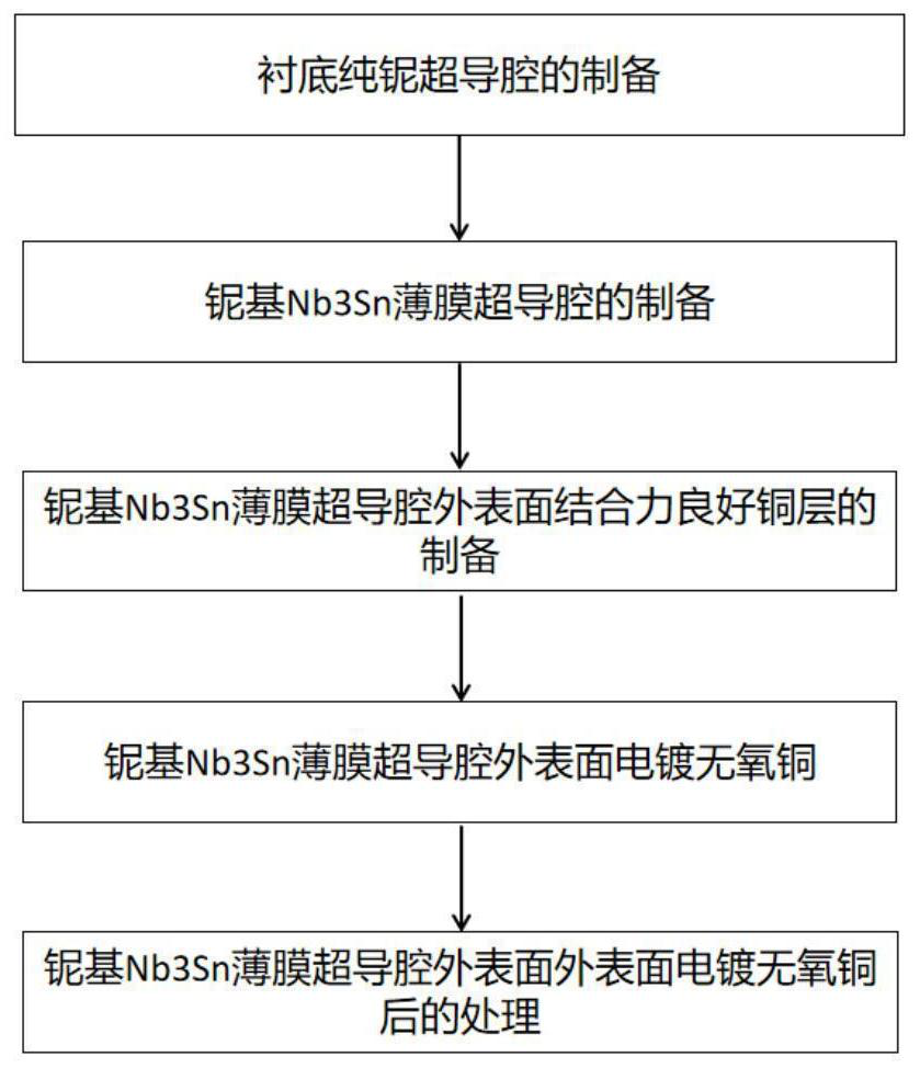
[0056] Embodiment 1, copper-based thick-walled Nb 3 Fabrication of Sn Thin Film Superconducting Cavities

[0057] 1. Niobium-based Nb 3 Fabrication of Sn Thin Film Superconducting Cavities

[0058] (1) Prepare a pure niobium superconducting cavity processed from a high-purity niobium plate with RRR>300 and a thickness of 2.0mm; the pure niobium superconducting cavity is prepared according to the method in the following literature: The International Linear ColliderTechnical Design Report 2013, Volume 3.I: Accelerator R&D;

[0059] (2) Carry out vacuum leak detection to the pure niobium superconducting cavity in step (1);

[0060] The pump set used for leak detection must be an oil-free pump set, and the leak rate of each sealing flange and weld of the pure niobium superconducting cavity must be lower than 1×10 -10 mbar L / s; this step of leak detection is to ensure that there are no leaks in the pure niobium superconducting cavity weld seam and each flange surface, to ensure...

Embodiment 2

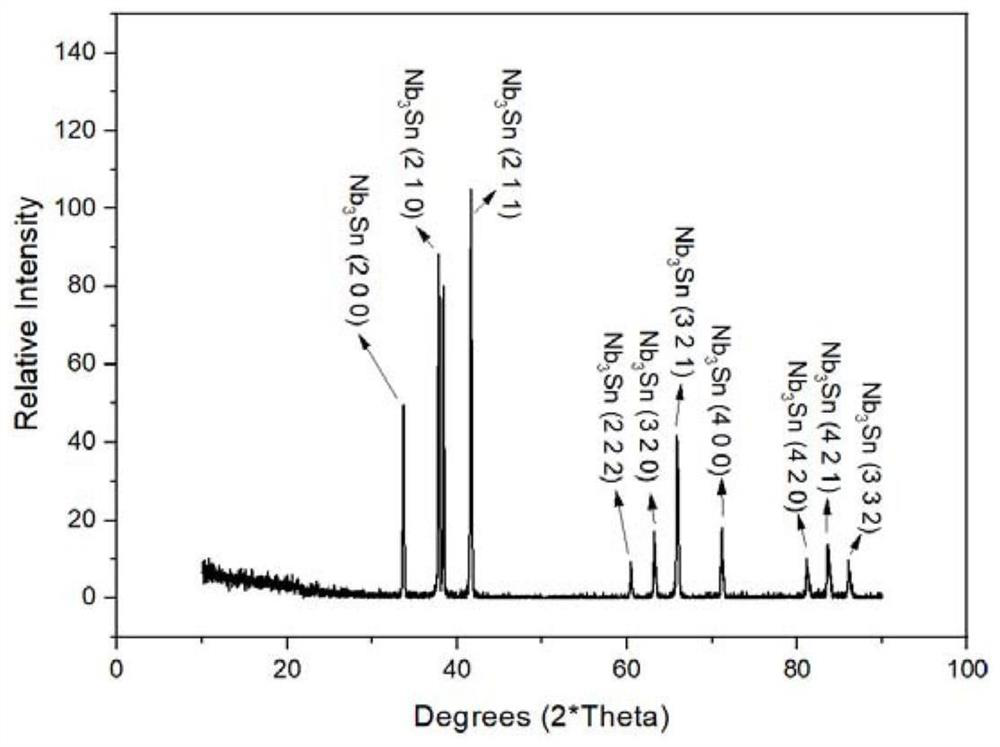
[0100] Embodiment 2, copper-based thick-walled Nb 3 Performance Test of Sn Thin Film Superconducting Cavity

[0101] The copper-based thick-walled Nb prepared in Example 1 3 The Sn thin film superconducting cavity has been tested as follows: 1. X-ray diffraction (see image 3 ) analysis showed that the grown Nb 3 Sn thin films contain only highly pure Nb 3 The Sn phase, without any other impurity phase, exhibits the high quality of the film. 2.4.2K~2K RF performance test at low temperature: 1. The test found that the Lorentz detuning coefficient LFD before the copper plating layer was -2.7182Hz / (MV / m) 2 , the influence of liquid helium pressure fluctuations on its frequency is df / dp=-102.77Hz / mbar, when its outer surface is electroplated with a copper layer with a thickness of 9mm, its Lorentz detuning coefficient is reduced to -0.6368Hz / (MV / m) 2 , df / dp=-18.7Hz / mbar, the mechanical stability is significantly improved (see Figure 4 ); 2. After electroplating the coppe...


PUM

PropertyMeasurementUnit
thicknessaaaaaaaaaa
thicknessaaaaaaaaaa
concentrationaaaaaaaaaa

Abstract

The invention discloses a copper-based thick-wall Nb3Sn thin film superconducting cavity and a preparation method thereof, and belongs to the technical field of superconducting. The invention discloses the preparation method of the copper-based thick-wall Nb3Sn thin film superconducting cavity, which comprises the following steps: (1) preparing a niobium-based Nb3Sn thin film superconducting cavity from a pure niobium superconducting cavity by adopting a tin vapor diffusion method; (2) depositing a copper layer on the outer surface of the niobium-based Nb3Sn thin film superconducting cavity; and (3) electroplating oxygen-free copper on the outer surface of the niobium-based Nb3Sn thin film superconducting cavity deposited with the copper layer to obtain the copper-based thick-wall Nb3Sn thin film superconducting cavity. According to the preparation method of the invention, the copper-based thick-wall Nb3Sn thin film superconducting cavity is prepared on the outer surface of the niobium-based Nb3Sn thin film superconducting cavity in a mode of electroplating oxygen-free copper, and the defect that a high-quality Nb3Sn thin film cannot be generated due to the low melting point of copper is successfully overcome; and the electroplated oxygen-free copper is high in density, low in porosity and small in thermal reaction.

Description

technical field [0001] The invention relates to the field of superconducting technology, in particular to a copper-based thick-walled Nb 3 Sn thin film superconducting cavity and its preparation method. Background technique [0002] Reducing manufacturing and operating costs is an urgent need for the development of large scientific devices based on RF superconducting accelerators; stable operation is a key physical problem and an important limiting factor for current and future applications of high-energy, high-intensity RF superconducting accelerators. The core component of the RF superconducting accelerator is the RF superconducting accelerating resonant cavity (hereinafter referred to as the superconducting cavity). The current superconducting cavity is mainly made of high-purity niobium material with RRR (residual resistivity ratio, which characterizes the purity of the material) > 300. (called: pure niobium superconducting cavity), and limited by the low thermal con...

Claims


Application Information

Patent Timeline
Patent Type & Authority Applications(China)
IPC IPC(8): C23C10/08C23C4/131C25D3/38C23C22/24C23G1/10
CPCC23C10/08C23C4/131C25D3/38C23C22/24C23G1/106
Inventor 杨自钦何源游志明郭浩熊平然张军辉张生虎
Owner INST OF MODERN PHYSICS CHINESE ACADEMY OF SCI
Why Eureka
Try Eureka