Preparation method of copper-based thick-wall niobium-based superconducting cavity

A superconducting cavity and copper-based technology, which is applied in the field of superconducting, can solve the problems that cannot be widely used, the grain size is small, and the RF performance of copper-niobium sputtering film cavity cannot reach that of pure niobium superconducting cavity.

Active Publication Date: 2021-09-10
INST OF MODERN PHYSICS CHINESE ACADEMY OF SCI
View PDF7 Cites 2 Cited by
  • Summary
  • Abstract
  • Description
  • Claims
  • Application Information

AI Technical Summary

Problems solved by technology

However, limited by the preparation process, the grain size of the sputtered niobium film is small, accompanied by limiting factors such as weak connection of grain boundaries and weak coupling of grain boundaries, so that the radio frequency performance of the copper niobium sputtered thin film cavity cannot reach that of a pure niobium superconducting cavity level, cannot be widely used in current large scientific devices of radio frequency superconducting accelerators

Method used


Image

  • Preparation method of copper-based thick-wall niobium-based superconducting cavity
  • Preparation method of copper-based thick-wall niobium-based superconducting cavity
  • Preparation method of copper-based thick-wall niobium-based superconducting cavity

Examples


Embodiment 1

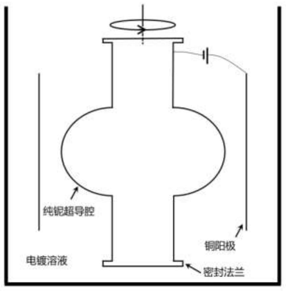
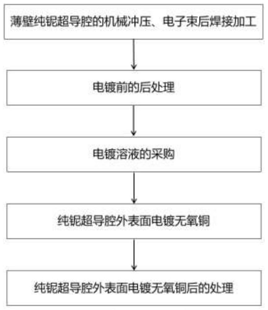
[0049] Example 1. Preparation of copper-based thick-walled pure niobium superconducting cavity by electroplating oxygen-free copper on the outer surface

[0050] 1. Mechanical stamping and post-electron beam welding of thin-walled pure niobium superconducting cavities are mainly to obtain substrate niobium cavities for copper plating on the outer surface. The main process includes:

[0051] ① Using high-purity niobium materials with RRR>300 and a thickness of 1.5-2.5mm, the thin-walled superconducting cavity parts and bundle tubes of the required shape are produced through stamping dies. The use of high-purity niobium plates of 1.5-2.5mm is to reduce the The wall thickness of the guide cavity is used to reduce the thermal resistance of the niobium material, and the niobium-titanium alloy material is used to process the flange that is connected to the bundle tube with a lathe;

[0052] ②Use an ultrasonic cleaning device to perform ultrasonic cleaning on the parts completed in s...


PUM

PropertyMeasurementUnit
thicknessaaaaaaaaaa
thicknessaaaaaaaaaa
lengthaaaaaaaaaa

Abstract

The invention discloses a preparation method of a copper-based thick-wall niobium-based superconducting cavity by electroplating oxygen-free copper on the outer surface. The method comprises the following steps: 1) carrying out mechanical stamping and electron beam welding processing on the thin-wall pure niobium superconducting cavity; 2) pretreating before electroplating of a pure niobium superconducting accelerating cavity, such as high-temperature degassing, inner and outer surface BCP polishing and ultrasonic cleaning; (3) preparing an oxygen-free copper electroplating solution; 4) electroplating oxygen-free copper on the outer surface of the pure niobium superconducting accelerating cavity; and (5) post-processing after electroplating the oxygen-free copper on the outer surface of the pure niobium superconducting accelerating cavity. The copper-based thick-wall niobium-based superconducting cavity developed by the invention is high in oxygen-free copper layer density, low in porosity, small in thermal reaction, large in copper wall thickness tolerance, low in batch production cost, capable of remarkably improving the mechanical stability and the thermal stability of the superconducting cavity on the premise of ensuring that the radio frequency performance of the copper-based thick-wall niobium-based superconducting cavity is not lower than the level of a pure niobium superconducting cavity; and suitable for large scientific devices based on the radio frequency superconducting accelerator technology.

Description

technical field [0001] The invention relates to the field of superconducting technology, in particular to a method for preparing a copper-based thick-walled niobium-based superconducting cavity by electroplating oxygen-free copper on the outer surface. Background technique [0002] The superconducting accelerating cavity used in the current radio frequency superconducting accelerator mainly adopts high-purity niobium plates with RRR (residual resistivity ratio, which characterizes the purity of the material) > 300 through mechanical stamping and electron beam welding. However, limited by the low thermal conductivity of niobium materials at operating temperatures of 4.2K or 2K, the wall thickness of pure niobium superconducting cavities generally does not exceed 3-4mm. On the one hand, the pure niobium superconducting cavity with a wall thickness of 3-4mm has poor mechanical stability and is sensitive to external disturbances such as microphonic noise, Lorentz detuning, an...

Claims


Application Information

Patent Timeline
Patent Type & Authority Applications(China)
IPC IPC(8): C25D3/38C25D5/38C25D7/04C23C4/131C23G1/10H05H7/20
CPCC25D3/38C25D5/38C25D7/04C23C4/131C23G1/106H05H7/20
Inventor 杨自钦何源路明皇世春吴安东郭浩谭腾
Owner INST OF MODERN PHYSICS CHINESE ACADEMY OF SCI
Why Eureka
Try Eureka