SE double-sided PERC battery adopting MBB main gate structure and preparation method of SE double-sided PERC battery
A grid structure and battery technology, applied in circuits, photovoltaic power generation, electrical components, etc., can solve the problem of low photoelectric conversion utilization rate, and achieve the effects of improving photoelectric conversion utilization rate, improving open circuit voltage, and increasing system power generation gain.
- Summary
- Abstract
- Description
- Claims
- Application Information
AI Technical Summary
Problems solved by technology
Method used
Image
Examples
Embodiment 1
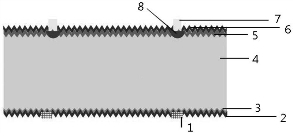
[0031] like figure 1 As shown, this embodiment provides a SE double-sided PERC battery adopting MBB busbar structure, comprising a silicon substrate 4 made of textured surface, and the back surface of the silicon substrate 4 is deposited with a back passivation layer 3 and a back subtraction layer in sequence. The reflection passivation protection film layer 2, the surface of the back anti-reflection passivation protection film layer 2 is screen-printed with multi-busbar rear electrode patterns and laser grooves, the grooves are provided with grid electrodes 1, and the front surface of the silicon substrate 4 is deposited with N N-type doped layer 5 and front anti-reflection passivation protective film layer 6, N-type doped layer 5 is provided with N+ type heavily doped region 8, the surface of front anti-reflection passivation protective film layer 6 is screen-printed with multi-busbar front electrode Figure, the front electrode of the multi-busbar battery is provided with an...
Embodiment 2
[0038] A method for preparing an SE double-sided PERC battery using an MBB busbar structure, characterized in that it comprises the following steps:
[0039] Step 1, using a compound chemical etching solution to perform pre-cleaning and surface texturing of the silicon substrate;
[0040] Step 2. Place the silicon substrate in step 1 in a tubular diffusion furnace at 840°C to 870°C, diffuse the silicon substrate with a POCl3 liquid source, and produce high-impurity Concentrated PSG layer and 160±8Ω sheet resistance, the uniformity of front impurity diffusion concentration is less than 5%;
[0041] Step 3, using laser irradiation with a wavelength of 532nm, designing an SE laser doping pattern according to the front electrode pattern of the multi-busbar battery, performing localized laser ablation, and realizing heavy doping of phosphorus in the irradiation area of the silicon wafer. Form an N-type high-concentration emitter, and prepare a preliminary selective emitter junct...
PUM
| Property | Measurement | Unit |
|---|---|---|
| thickness | aaaaa | aaaaa |
| thickness | aaaaa | aaaaa |
Abstract
Description
Claims
Application Information
 - R&D
- Intellectual Property
- Life Sciences
- Materials
- Tech Scout
- Unparalleled Data Quality
- Higher Quality Content
- 60% Fewer Hallucinations
Browse by: Latest US Patents, China's latest patents, Technical Efficacy Thesaurus, Application Domain, Technology Topic, Popular Technical Reports.
© 2025 PatSnap. All rights reserved.Legal|Privacy policy|Modern Slavery Act Transparency Statement|Sitemap|About US| Contact US: help@patsnap.com

