Method for preparing nano-composite conductive thin film for photovoltaic cell

A nano-composite, conductive thin film technology, used in photovoltaic power generation, circuits, electrical components, etc., can solve the problems of limited anti-reflection effect of a single silicon oxide-based anti-reflection coating, surface electrostatic dust adsorption, etc., to achieve maintenance-free and Long-term operation, high transmittance, and the effect of improving photoelectric conversion efficiency and utilization rate

Inactive Publication Date: 2015-11-11
XIAN UNIV OF TECH
View PDF3 Cites 2 Cited by
  • Summary
  • Abstract
  • Description
  • Claims
  • Application Information

AI Technical Summary

Problems solved by technology

[0006] The purpose of the present invention is to provide a method for preparing a nanocomposite conductive film for photovoltaic cells, which solves the limitations of the existing single silicon oxide-based anti-reflection film coating with limited anti-reflection effect and surface electrostatic dust adsorption, and at the same time extends its absorption. Wavelength to ultraviolet band, stabilize the working point of silicon devices in solar cells, fundamentally improve its photoelectric conversion efficiency, improve and enhance the engineering applicability of current solar cells, and realize maintenance-free and long-term work

Method used


Image

  • Method for preparing nano-composite conductive thin film for photovoltaic cell
  • Method for preparing nano-composite conductive thin film for photovoltaic cell
  • Method for preparing nano-composite conductive thin film for photovoltaic cell

Examples


Embodiment 1

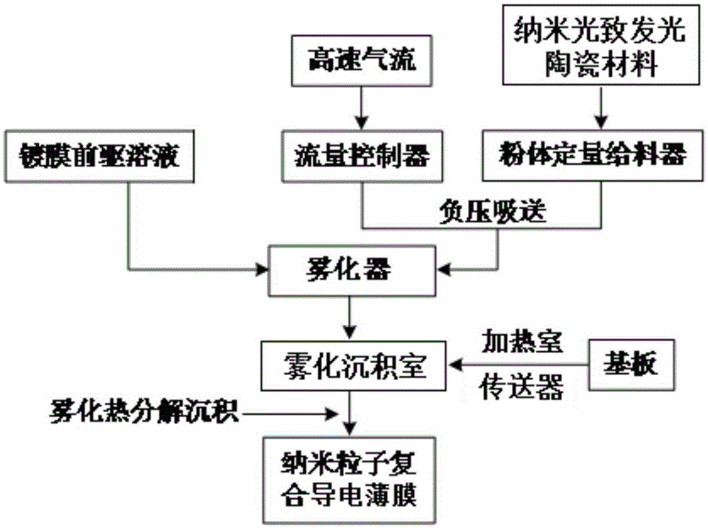
[0049] Step 1, prepare deposition aerosol:

[0050] 1.1 Europium-doped vanadium phosphate nano ceramic powder (Eu:YP x V (1-x) o 4 , x=0.4~0.6, commercially available, 15nm~20nm) put into the powder quantitative feeder, control the feeding speed to 0.1g / min~0.22g / min, adopt high-speed airflow siphon negative pressure to make nano photoluminescence The ceramic material forms an atomized air flow, and the air flow rate is controlled to be 1L / min~1.5L / min;

[0051] 1.2 The atomizing airflow atomizes the ATO (antimony-doped tin oxide) solution (concentration: 10wt% to 12wt%) in the water system in the atomizer to form a deposition aerosol, which is passed into the atomization deposition chamber.

[0052] Step 2, nanoparticle composite film deposition:

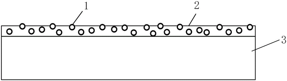
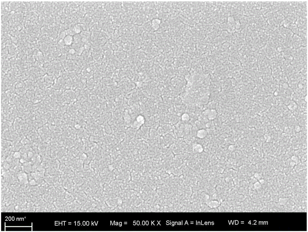
[0053] Heat the ultra-clear glass substrate for photovoltaic cells to 480°C-500°C in the heating chamber, send it into the atomization deposition chamber through the conveyor, and deposit the deposition mist on the substrate fo...

Embodiment 2

[0055] Step 1, prepare deposition aerosol:

[0056] 1.1 Europium-doped yttrium vanadate nano ceramic powder (Eu:YVO 4 , commercially available, 30nm ~ 40nm) into the powder quantitative feeder, control the feeding speed of 1.8g / min ~ 2g / min, use the high-speed airflow siphon negative pressure to make the nano photoluminescent ceramic material form an atomized airflow, Control the flow rate of airflow to 6L / min~7L / min;

[0057] 1.2 The atomizing gas flow atomizes the FTO (fluorine-doped tin oxide) solution (concentration: 15wt%-20wt%) of the water system in the atomizer to form a deposition aerosol, which is passed into the atomization deposition chamber.

[0058] Step 2, nanoparticle composite film deposition:

[0059] Heat the ultra-white glass substrate for photovoltaic cells to 500°C-520°C in the heating chamber, and send it into the atomization deposition chamber through the conveyor, so that the deposition mist is deposited on the substrate for 5-10s, and a photovoltaic...

Embodiment 3

[0061] Step 1, prepare deposition aerosol:

[0062] 1.1 Europium-doped yttrium vanadate nano ceramic powder (Eu:YVO 4 , commercially available, 20nm ~ 30nm) into the powder quantitative feeder, control the feeding speed of 0.5g / min ~ 0.8g / min, use high-speed airflow siphon negative pressure to make the nano-photoluminescent ceramic material form an atomized airflow , control the air flow rate to 4L / min~5L / min;

[0063] 1.2 Atomizing air flow ATO (antimony-doped tin oxide) solution (concentration: 15wt%-17wt%) in isopropanol system is atomized in the atomizer to form deposition aerosol, which is passed into the atomization deposition chamber.

[0064] Step 2, nanoparticle composite film deposition:

[0065] Heat the ultra-clear glass substrate for photovoltaic cells to 640°C-650°C in the heating chamber, send it into the atomization deposition chamber through the conveyor, and deposit the deposition mist on the substrate for 18-20s to obtain a photovoltaic cell with a thickne...


PUM

PropertyMeasurementUnit
particle diameteraaaaaaaaaa
thicknessaaaaaaaaaa
thicknessaaaaaaaaaa

Abstract

The invention discloses a method for preparing a nano-composite conductive thin film for a photovoltaic cell, and specifically includes: depositing nanometer photoluminescence material deposition aerial fog wrapped by a coating precursor solution on a heated substrate, thereby obtaining the nano-composite conductive thin film for a photovoltaic cell. The method can convert an ultraviolet light wave band of sunlight to visible light by adoption of red fluorescent powder, so that photoelectric conversion of a silicon device in a photovoltaic cell is convenient, and the photoelectric conversion utilization rate is improved by 1% to 1.5%; electrical conductivity of the transparent conductive thin film is utilized, transmittance is improved and high transmittance in long-term operation is maintained, and photoelectric conversion efficiency and the utilization rate under actual working conditions are improved; and an infrared reflection characteristic of the transparent conductive film is utilized, thereby reducing a heat effect, stabilizing an operating point of a silicon device in a solar cell, improving photoelectric conversion efficiency, effectively improving engineering applicability of a solar cell at present, and realizing a maintenance-free effect and long-period working.

Description

technical field [0001] The invention belongs to the technical field of photoelectric thin film preparation, and relates to a preparation method of a nanocomposite conductive thin film for photovoltaic cells. Background technique [0002] In recent years, the application of glass deep-processing products characterized by high light transmittance in photovoltaic (solar) cell windows has shown increasingly strong market demand and technical advantages, forming a representative glass deep-processing industry direction. [0003] With the popularization of solar photovoltaic cells from the military and aerospace fields into the fields of industry, commerce, agriculture, communications, household appliances, and public facilities, their convenience and flexibility are especially suitable for remote areas, mountains, deserts, islands, and rural areas. Show strong market demand. However, as one of its key components, window glass requires high transmittance in the visible and near-i...

Claims


Application Information

Patent Timeline
Patent Type & Authority Applications(China)
IPC IPC(8): H01L31/18H01L31/0232
CPCH01L31/02322H01L31/02327H01L31/1884Y02E10/52Y02P70/50
Inventor 张卫华赵彦珍洪繁陈源清
Owner XIAN UNIV OF TECH
Why Eureka
Try Eureka