Terahertz wave modulator based on magnetic tunnel junction and preparation method of terahertz wave modulator

A magnetic tunnel junction and modulator technology, which is applied in the fields of magnetic field controlled resistors, the manufacture/processing of electromagnetic devices, material selection, etc., can solve the problems of narrow modulation spectrum, difficult to meet requirements, and small depth, etc. The effect of wide range, high modulation depth and low power consumption

Pending Publication Date: 2021-09-24
UNIV OF SHANGHAI FOR SCI & TECH
View PDF8 Cites 1 Cited by
  • Summary
  • Abstract
  • Description
  • Claims
  • Application Information

AI Technical Summary

Problems solved by technology

Existing terahertz modulation devices have narrow modulation spectrum and small depth, making it difficult to achieve continuous adjustment
T

Method used


Image

  • Terahertz wave modulator based on magnetic tunnel junction and preparation method of terahertz wave modulator
  • Terahertz wave modulator based on magnetic tunnel junction and preparation method of terahertz wave modulator
  • Terahertz wave modulator based on magnetic tunnel junction and preparation method of terahertz wave modulator

Examples


preparation example Construction

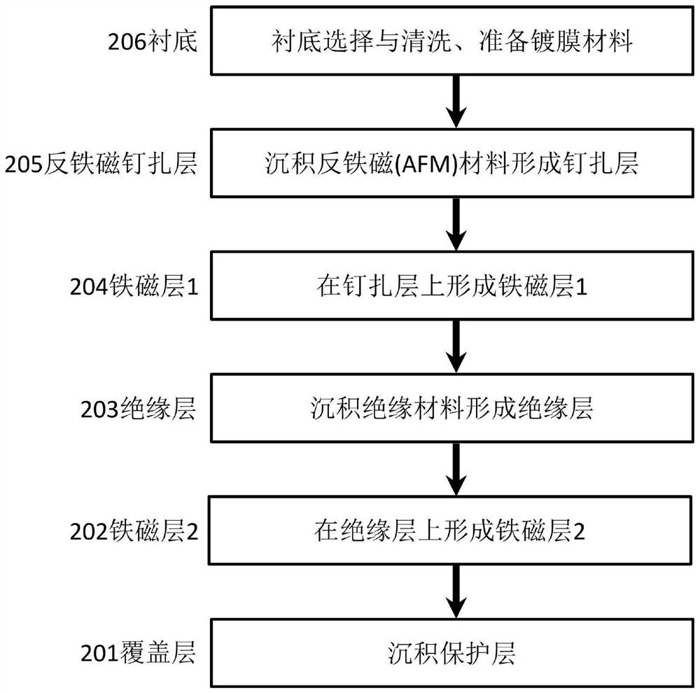
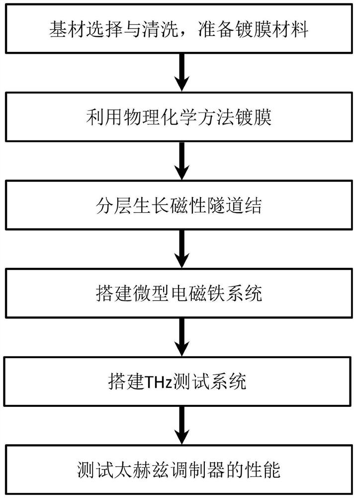
[0040] A preparation method of a terahertz wave modulator based on a magnetic tunnel junction, using physical or chemical coating methods, successively coating a multi-layer magnetic metal film and a non-magnetic metal film on a substrate to form a composite film structure; an external small An electromagnet; by controlling the current, the regulation of the amplitude of the terahertz radiation is realized, including the following steps:

[0041] S206, selecting and cleaning the substrate, and preparing materials for coating;

[0042] S205, depositing an antimagnetic material on the substrate to form an antiferromagnetic pinning layer 105;

[0043] S204, forming a first ferromagnetic layer 104 on the antiferromagnetic pinning layer 105 above S205;

[0044] S203, depositing an insulating material on the first ferromagnetic layer 104 in step S204 to form an insulating layer 103;

[0045] S202, forming a second ferromagnetic layer 102 on the insulating layer 103 in step S203;

...

Embodiment 1

[0049] see Figure 1~2 , the terahertz wave emitter is composed of a substrate substrate and a magnetic tunnel junction plated on the substrate. From the substrate to the top: 105 antiferromagnetic pinning layer (IrMn-10nm), 104 ferromagnetic layer (CoFeB-3nm), 103 insulating layer (MgO-1.9nm), 102 ferromagnetic layer (CoFeB-3nm) , 101 cover layer (Ta-5nm). Wherein the ferromagnetic layer has an in-plane magnetization direction. The given thickness is a commonly used thickness, and changing different thicknesses can greatly change the background transmittance of terahertz waves. In addition, buffer layers are often used to fill between layers to improve performance. Ru is commonly used, with a thickness of less than 1nm. Use commonly used physical and chemical coating methods, such as magnetron sputtering, chemical vapor deposition, molecular beam epitaxy, etc.

[0050] image 3 The overall test scheme of the terahertz modulator is given.

[0051] Figure 4 It is a sche...


PUM

PropertyMeasurementUnit
Thicknessaaaaaaaaaa
Thicknessaaaaaaaaaa
Thicknessaaaaaaaaaa

Abstract

The invention discloses a terahertz wave modulator based on a magnetic tunnel junction. The terahertz wave modulator comprises a substrate and a composite film heterostructure fixed on the substrate, the composite film heterostructure comprises an antiferromagnetic pinning layer fixedly connected to a substrate, a first ferromagnetic layer fixed on the antiferromagnetic pinning layer, an insulating layer fixed on the first ferromagnetic layer, a second ferromagnetic layer fixed on the insulating layer and a covering layer fixed on the second ferromagnetic layer. According to the terahertz modulator, the working range is wide, the size is small, and large-amplitude modulation of terahertz waves can be achieved by using a weak magnetic field. And the terahertz wave modulator is compatible with a semiconductor process technology, and large-scale manufacturing can be conveniently realized.

Description

technical field [0001] The invention relates to the technical field of photoelectric functional devices, in particular to a terahertz wave modulator based on a magnetic tunnel junction and a preparation method thereof. Background technique [0002] Terahertz wave refers to the electromagnetic spectrum region between millimeter wave and infrared optics with a wavelength of 3mm-30μm and a corresponding frequency range of 0.1-10THz. After the development of technologies such as terahertz spectroscopy and imaging, terahertz science and technology have shown great application prospects. For terahertz wave spectroscopy and communication applications, terahertz waves need to be modulated. The modulation of the terahertz wave refers to changing the amplitude of the terahertz wave by using a modulating device. The existing terahertz modulation devices have narrow modulation spectrum and small depth, making it difficult to achieve continuous adjustment. Therefore, it is difficult t...

Claims


Application Information

Patent Timeline
IPC IPC(8): H01L43/08H01L43/10H01L43/12
CPCH10N50/01H10N50/85H10N50/10
Inventor 金钻明朱亦鸣彭滟庄松林倪洋洋
Owner UNIV OF SHANGHAI FOR SCI & TECH
Why Eureka
Try Eureka