
MEMS inertial sensor chip module and preparation method thereof

An inertial sensor and chip module technology, applied in instruments, electric solid state devices, semiconductor devices, etc., can solve the problems of volume contradiction, complex overall process, increase in chip volume, etc., to reduce packaging and integration costs, reduce integration volume, Improve the effect of app restrictions

Pending Publication Date: 2021-09-28
湖南天羿领航科技有限公司
View PDF0 Cites 0 Cited by
  • Summary
  • Abstract
  • Description
  • Claims
  • Application Information

AI Technical Summary

Problems solved by technology

[0002] Inertial sensors based on MEMS technology have the advantages of light weight, low cost, small size, and mass production, and have extremely broad application and development prospects in civil, aerospace, and military fields; Ceramic shell package, plastic package, ceramic substrate COB package and other first-level packaging forms, and then adopt surface mount technology (SMT), chip direct mount technology (DCA), through-hole mount technology (THT) and other technologies, together with passive components Installed together on PCB or other substrates (secondary packaging form) to become a component or a complete machine, the overall process is relatively complicated; or use low-temperature solder paste for surface mounting, but it is not conducive to subsequent process development
[0003] In the process of first-level packaging and second-level packaging, due to the large difference in coefficient of thermal expansion (CTE) between materials, thermal stress and welding stress are easily caused, and MEMS inertial sensor chips are easily affected by packaging stress and welding stress, especially Full-temperature characteristic index; in single-chip integrated packaging, ASIC and MEMS chips are often stacked, and the heat generated by ASIC will also affect the output performance of MEMS; in addition, ceramic shells, ceramic substrates, plastic shells, etc. are molded or processed by themselves The cost is relatively high, it is not versatile, and the relative chip volume is obviously increased several times, or even larger, and the volume contradiction is particularly obvious in the application of inertial measurement unit (IMU) integration

Method used


Image

  • MEMS inertial sensor chip module and preparation method thereof
  • MEMS inertial sensor chip module and preparation method thereof
  • MEMS inertial sensor chip module and preparation method thereof

Examples


Embodiment Construction

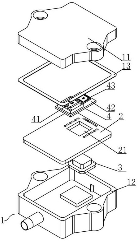
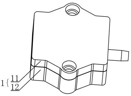
[0036] Such as figure 1 , figure 2 with image 3 As shown, the MEMS inertial sensor chip module of the present embodiment includes a housing 1, and the housing 1 is respectively fixed with a PCB board 2 and a metal support column 3, and the metal support column 3 is supported with a MEMS inertial sensor chip assembly 4, and the MEMS inertial sensor The connecting terminals on the chip component 4 are connected to the connecting terminals on the PCB 2 through metal wires.

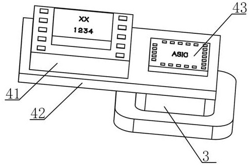
[0037] Such as figure 1 , figure 2 with Figure 4 As shown, in this embodiment, the MEMS inertial sensor chip assembly 4 includes a MEMS inertial sensor chip 41 and a substrate 42 with the same thermal expansion coefficient as the MEMS inertial sensor chip 41, the MEMS inertial sensor chip 41 is fixed on the substrate 42, and the substrate 42 supports and fixes On the end face of the metal support column 3.

[0038] It should be noted that, the MEMS inertial sensor chip assembly 4 can adopt a monocry...


PUM


Abstract

The invention discloses an MEMS inertial sensor chip module and a preparation method thereof. The MEMS inertial sensor chip module comprises a shell, a PCB and a metal support column are fixed on the shell, an MEMS inertial sensor chip assembly is supported on the metal support column, and connecting terminals on the MEMS inertial sensor chip assembly are connected with connecting terminals on the PCB through metal wires. According to the invention, a primary packaging process is not needed, the packaging and integration cost is greatly reduced, the integration volume is reduced, the thermal stress caused by surface mounting is avoided, rapid heat conduction can be realized, various performance indexes of the MEMS inertial sensor chip level can be maintained, the application limitation of the prior art on an MEMS inertial sensor chip can be improved, and the influence of the thermal stress of the first-stage packaging or the second-stage packaging on the system integration application is avoided.

Description

technical field [0001] The invention relates to semiconductor devices, in particular to a MEMS inertial sensor chip module and a preparation method thereof, which are used for integrated assembly of inertial sensor chips such as MEMS gyroscopes and MEMS accelerometers. Background technique [0002] Inertial sensors based on MEMS technology have the advantages of light weight, low cost, small size, and mass production, and have extremely broad application and development prospects in civil, aerospace, and military fields; Ceramic shell package, plastic package, ceramic substrate COB package and other first-level packaging forms, and then adopt surface mount technology (SMT), chip direct mount technology (DCA), through-hole mount technology (THT) and other technologies, together with passive components Installed together on a PCB or other substrates (secondary packaging form) to become a component or a complete machine, the overall process is relatively complicated; or surface...

Claims


Application Information

Patent Timeline
Patent Type & Authority Applications(China)
IPC IPC(8): B81B7/00B81B7/02B81C1/00
CPCB81B7/0032B81B7/0045B81B7/007B81B7/0093B81B7/02B81C1/0023B81C1/00261B81C1/00325B81C1/00301B81B2201/0228B81B2201/0235
Inventor 虢晓双杨靖张新凯熊亮黎傲雪彭健
Owner 湖南天羿领航科技有限公司
Features
  • Generate Ideas
  • Intellectual Property
  • Life Sciences
  • Materials
  • Tech Scout
  • Unparalleled Data Quality
  • Higher Quality Content
  • 60% Fewer Hallucinations
Learn More