OLED display structure and display device

A technology of display structure and organic light-emitting layer, applied in electrical components, diodes, electro-solid devices, etc., can solve the problems of increasing process difficulty, increasing pixel layer thickness, reducing device life, etc., so as to improve the manufacturing process difficulty and increase effective Absorption, the effect of improving the absorption rate

Pending Publication Date: 2021-09-28
XIANYANG CAIHONG OPTOELECTRONICS TECH CO LTD
View PDF0 Cites 4 Cited by
  • Summary
  • Abstract
  • Description
  • Claims
  • Application Information

AI Technical Summary

Problems solved by technology

In addition, ultraviolet light will also have adverse effects on the internal materials of the device, reducing the life of the device
In the prior art, ultraviolet light and blue light absorbers are mostly added to one or more components of the color filter, and the absorber is usually added in the production of photoresist materials. This method will increase the thickness of the pixel layer , the preparation process is relatively complicated, which greatly increases the production cost of the display device
[0005] In the existing OLED display structure, such as figure 2 As shown, in order to improve the blue light absorption rate of pixels, the method of increasing the thickness of the pixel layer is usually used, and the thickness of the black matrix needs to be increased accordingly, and the number of quantum dot photoresists will also increase, thereby increasing the difficulty of the process and improving the manufacturing process. cost

Method used


Image

  • OLED display structure and display device
  • OLED display structure and display device
  • OLED display structure and display device

Examples


Embodiment 1

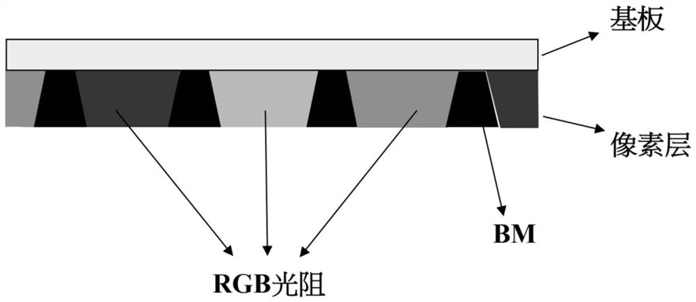
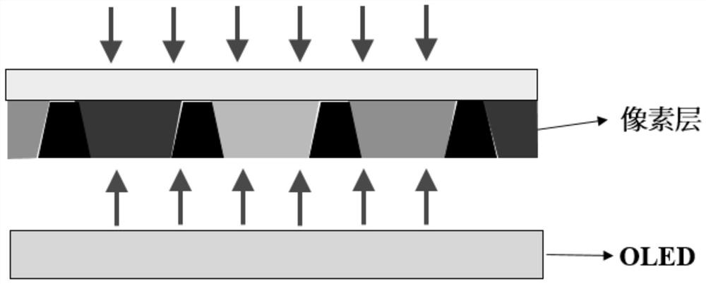
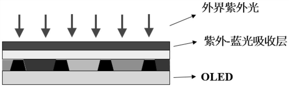
[0033] Such as image 3 , Figure 4 As shown, an OLED display structure provided in an embodiment of the present disclosure includes:

[0034] organic light emitting layer (OLED) 10;

[0035] A color filter layer 402, on which an array substrate (COA) and color pixel units are integrated, located on the organic light-emitting layer;

[0036] A light-absorbing layer (ultraviolet-blue light absorbing layer) 50, used to absorb external ultraviolet light and blue light, is located on the color filter layer;

[0037] Wherein, the color pixel unit includes: a red pixel unit, a green pixel unit and a blue pixel unit.

[0038] In this example, if Figure 5 As shown, there is a blue organic light-emitting material on the organic light-emitting layer, which is used to emit light in the blue light band; a blue-light absorption layer 401 is also arranged between the organic light-emitting layer and the color filter layer, which is used to absorb the blue light. Part of the blue light...

Embodiment 2

[0051] On the basis of the first embodiment, an embodiment of the present invention further provides a display device, including the OLED display structure described in any one of the preceding items.


PUM

PropertyMeasurementUnit
thicknessaaaaaaaaaa

Abstract

The embodiment of the invention discloses an OLED display structure. The OLED display structure comprises an organic light-emitting layer, a color filter layer and a light absorption layer; an array substrate, a red pixel unit, a green pixel unit and a blue pixel unit are integrated on the color filter layer, and the color filter layer is located on the organic light-emitting layer; and the light absorption layer is used for absorbing external ultraviolet light and blue light and is positioned on the color filter layer, wherein the red pixel unit, the green pixel unit and the blue pixel unit are integrated on the array substrate. By arranging the light absorption layer and (or) a blue light absorption layer in the OLED display structure, on the premise that the thickness of the pixel layer is not increased and the difficulty of the manufacturing process is improved, the absorption rate of OLED blue light is improved, and the damage of external ultraviolet light and blue light to a COA layer material is reduced, so that the problem that the color gamut is reduced due to mixed output of blue light, green light and red light is avoided, effective absorption of blue light emitted by the OLED is increased, and harm of the blue light to human eyes is reduced to a great extent.

Description

technical field [0001] The present disclosure relates to the display field, and in particular to an OLED display structure and a display device. Background technique [0002] With the continuous improvement of people's living standards, the large-area, ultra-thin and flexible market requirements for healthy and intelligent display technologies for display panels and lighting systems will gradually become an urgent need for people's lives. Global LCD (Liquid-crystal display liquid crystal display) ) Panel demand is stagnant, facing the crisis of overcapacity. The rapid occupation of the market by new display technologies has become the focus of research and development of major companies. Among them, organic light-emitting diodes or organic light-emitting diodes (organic light-emitting diodes, OLEDs) have low driving voltage, high efficiency, fast response, and wide viewing angles. , Thin and large-area, and flexible display can be realized, which has attracted extensive att...

Claims


Application Information

Patent Timeline
Patent Type & Authority Applications(China)
IPC IPC(8): H01L27/32H01L51/52
CPCH10K59/35H10K59/38H10K50/865
Inventor 蔡奇哲汪红
Owner XIANYANG CAIHONG OPTOELECTRONICS TECH CO LTD
Why Eureka
Try Eureka