Laser eutectic welding device for miniature LED chip and control substrate

A technology for LED chips and control substrates is applied in the field of laser eutectic welding devices for micro LED chips and control substrates, which can solve the problems of lowering the product qualification rate, labor consumption, damage to LED chips, etc., so as to reduce the process of adding solder and save production costs. , the effect of increasing the eutectic speed

Pending Publication Date: 2021-09-28
乙力国际股份有限公司
View PDF0 Cites 2 Cited by
  • Summary
  • Abstract
  • Description
  • Claims
  • Application Information

AI Technical Summary

Problems solved by technology

[0003] Micro LED will have great application prospects in the future, but the current manufacturing cost of Micro LED has seriously affected its commercialization process. The main reason is that the bottleneck of mass transfer technology still needs to be broken through. Eutectic soldering and single transfer severely limit the mass production process of Micro LED. Due to the higher resolution of Micro LED, a small Micro LED display contains a large number of LED chips, such as a 0.39-inch Micro LED display. , which contains about 2.4 million LED chips, if a single chip transfer method is used, it is particularly time-consuming and labor-intensive, and it is difficult to implement, and a single eutectic soldering will greatly reduce the product qualification rate. Crystal welding is to transfer one LED chip, heat the control substrate, and weld it with the control substrate. After the next LED chip is transferred, it will heat the control substrate as a whole, and connect the second LED chip with the control substrate. The control substrate is welded together, and the overall heating of the control substrate will cause the welding point of the first LED chip to melt
The problem of secondary and multiple melting occurred, which caused damage to the LED chip and seriously affected the product qualification rate

Method used


Image

  • Laser eutectic welding device for miniature LED chip and control substrate
  • Laser eutectic welding device for miniature LED chip and control substrate
  • Laser eutectic welding device for miniature LED chip and control substrate

Examples


Embodiment 1

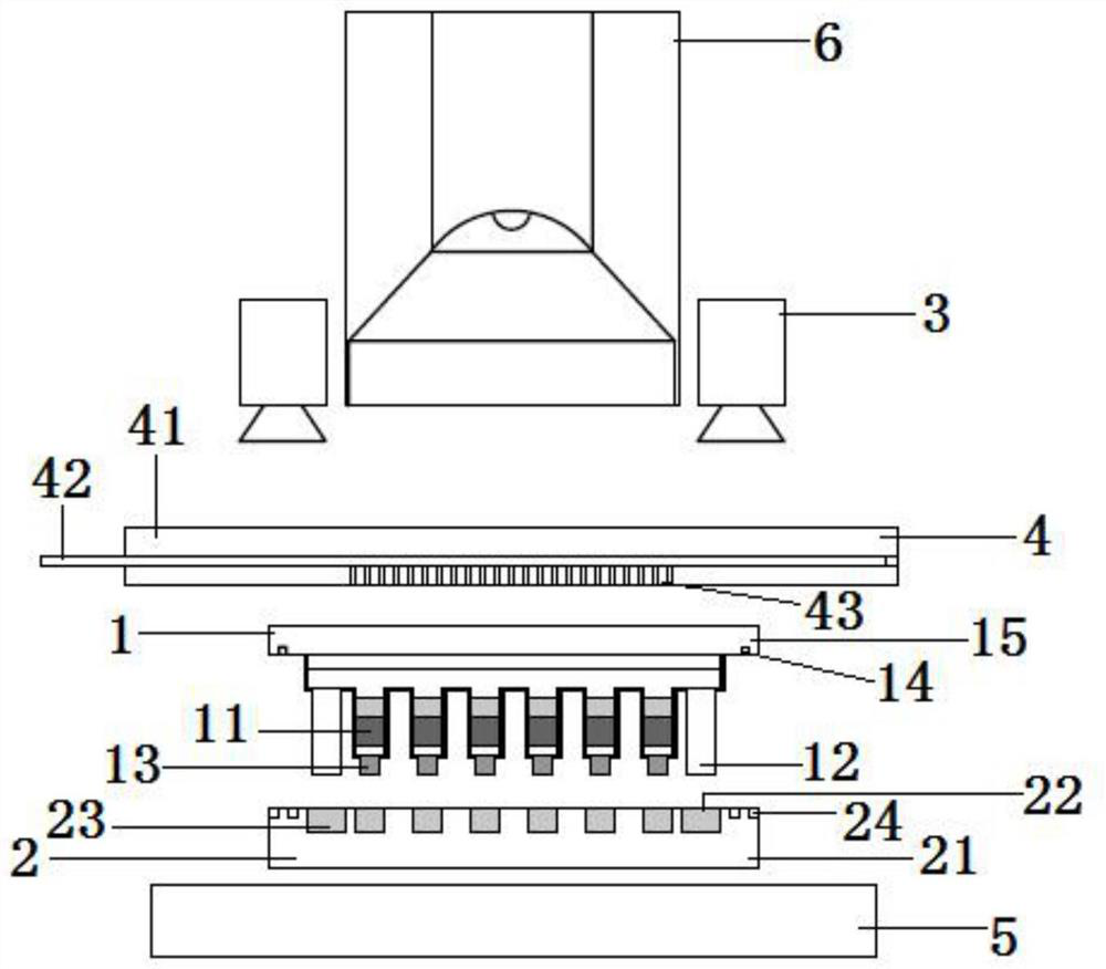
[0055] This embodiment provides a laser eutectic welding device for a micro LED chip and a control substrate, the purpose of which is to simultaneously weld multiple LED chips in the micro LED chip 1 and the control substrate 2 together by using a laser;

[0056] The micro LED chip 1 includes a chip substrate 15 and a plurality of LED chips 11 fixed on the chip substrate 15; a plurality of LED chips 11 have a common first negative electrode 12, and a plurality of LED chips 11 have independent a first positive electrode 13;

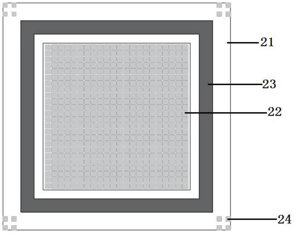
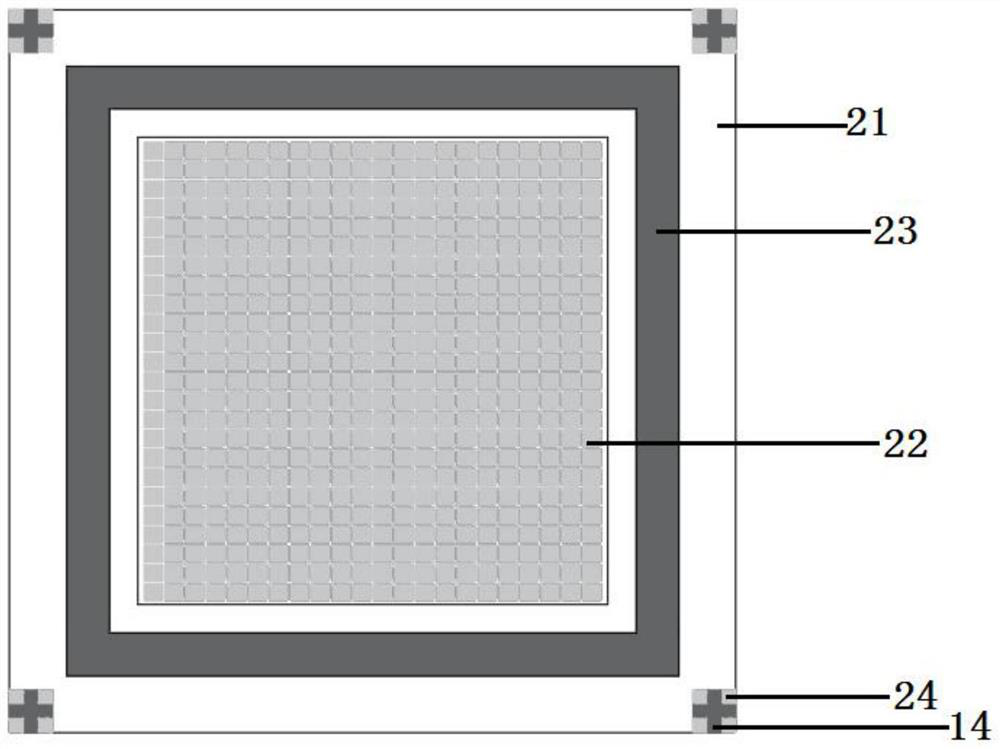
[0057] The control substrate 2 is located below the micro LED chip 1, and it includes a control substrate main body 21 and a plurality of second positive electrodes 22 and a second negative electrode 23 located on the control substrate main body 21;

[0058] The laser eutectic welding device includes:

[0059] a negative pressure adsorption unit 4, which is used to absorb the micro LED chip 1 and place it on the control substrate 2;

[0060] The laser em...


PUM


Abstract

The invention discloses a laser eutectic welding device for a miniature LED chip and a control substrate. A plurality of LED wafers in the miniature LED chip (1) and the control substrate (2) are welded together through laser. The laser eutectic welding device comprises a negative pressure adsorption unit (4) used for adsorbing the micro LED chip (1) and placing the micro LED chip (1) on the control substrate (2), and a laser emitting system (6) which is positioned above the micro LED chip (1) and is used for heating welding points of a plurality of first positive electrodes (13) and a plurality of second positive electrodes (22) as well as a first negative electrode (12) and a second negative electrode (23) by emitting laser to finish simultaneous eutectic welding. According to the device, the temperature of a heating area can be accurately controlled by adopting laser heating temperature, so that micro LED modular transfer eutectic welding is realized, and secondary melting of a single transfer eutectic welding point of the single Micro LED is avoided. Meanwhile, eutectic welding is transferred in an array mode through MicroLED modularization, the speed is high, and the eutectic speed is effectively increased.

Description

technical field [0001] The patent of the invention belongs to the field of micro-LED technology, and specifically relates to a laser eutectic welding device and method for a micro-LED chip and a control substrate. Background technique [0002] Micro LED (micro LED) technology is LED micro-matrix technology, which refers to a high-density picometer-level LED array integrated on a chip, which is widely used in display screens, visible light communications, smart portable devices and other fields. It has the advantages of stable performance and long life, and also continues the advantages of LED such as low power consumption, fast response, and strong contrast. At the same time, it also inherits the advantages of LED low power consumption, color saturation, fast response speed, and strong contrast. The brightness of Micro LED is 30 times higher than that of OLED, and the energy consumption is about 10% of LCD and 50% of OLED. [0003] Micro LED will have great application pros...

Claims


Application Information

Patent Timeline
Patent Type & Authority Applications(China)
IPC IPC(8): H01L33/00H01L33/62H01L21/683B23K26/21B23K26/70B23K37/04
CPCH01L33/62H01L33/0095H01L21/6838B23K26/21B23K26/702B23K37/0443H01L2933/0066
Inventor 林俊荣王宏吕河江
Owner 乙力国际股份有限公司
Why Eureka
Try Eureka