


Quick Research
Generate reliable direction feasibility study reports for your R&D in just a few steps.

Technical Q&A
Discover and master advanced knowledge NOW. Basics, ideas, possibilities, all at once.

Find Solutions
As an expert in R&D theories, this can generate solutions to your technical problems instantly.

Evaluate Feasibility
Analyze your overall solution with one click, know your potential R&D risks in advance.

Monitor Landscape
Get weekly tech updates, stay abreast of the latest tech innovations and key insights.
Processing method for regenerated light-transmitting blankmask and manufacturing method for blankmask
A technology of a light-transmitting substrate and a processing method, which is applied to manufacturing tools, laser welding equipment, ion implantation and plating, etc., can solve the problems of complex process and long-term operation, and achieve the effect of reducing manufacturing cost and realizing recyclability.
- Summary
- Abstract
- Description
- Claims
- Application Information
AI Technical Summary
Problems solved by technology
Method used
Image

Examples
Embodiment 1
[0045] Such as Figure 1 to Figure 4 As shown, this embodiment provides a processing method for regenerating a masked light-transmitting substrate, and the processing method includes the steps of:
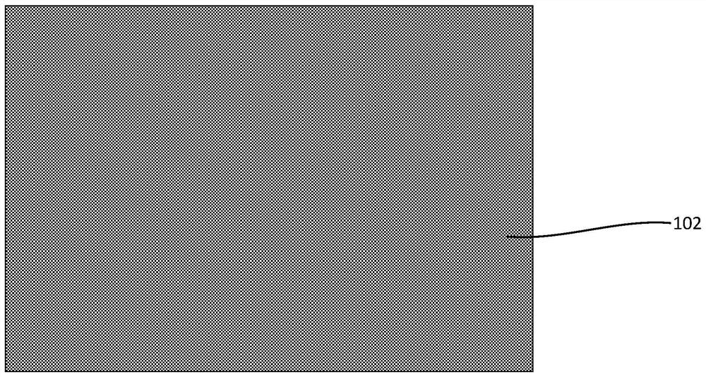
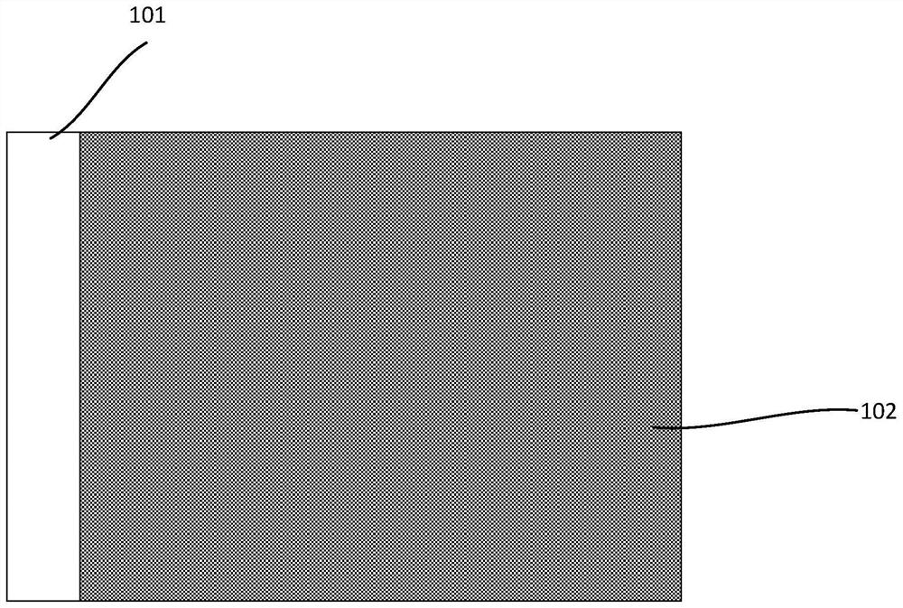
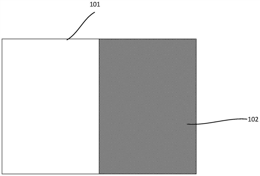
[0046] Such as figure 1 As shown, step 1) is performed first, and a mask base plate is provided, and the mask base plate includes a light-transmitting substrate 101 and a mask material layer 102 on the light-transmitting substrate 101 .
[0047] As an example, the transparent substrate includes one of a quartz substrate, a soda lime substrate, a borosilicate substrate, an aluminum silicate substrate, a silicon substrate, and a silicon carbide substrate, and the radial dimension of the transparent substrate 101 is between 1 Inch to 100 inches, thickness between 0.1mm and 200mm. For example, in this embodiment, the transparent substrate may be a quartz substrate, and its radial dimension may be 4 inches, 6 inches, 8 inches, 12 inches, etc.
[0048] The material of the mask materia...
Embodiment 2
[0060] Such as Figure 5 to Figure 9 As shown, the present embodiment provides a method for manufacturing a mask base, and the method for manufacturing includes the steps of:
[0061] Such as Figure 5 As shown, step 1) is firstly performed to provide a regenerated masked light-transmitting substrate manufactured by the processing method for regenerating a masked light-transmitting substrate described in Embodiment 1.
[0062] Such as Figure 6 As shown, step 2) is then performed to deposit a light-shielding film 202 on the light-transmitting substrate of the regenerated mask.
[0063] For example, the light shielding film 202 includes one of CrN, CrC and CrCN.
[0064] Specifically, in this embodiment, a light-shielding film 202 is deposited on the light-transmitting substrate of the regenerated mask through a magnetron sputtering process, wherein the inert gas introduction part of the sputtering device is injected with 20-80 SCCM of argon (Ar) and helium ( He) 20~80SCCM,...
Embodiment 3
[0074] Such as Figure 10As shown, this embodiment provides a method for manufacturing a mask base, and the basic steps of the manufacturing method are as in Embodiment 2, wherein, the difference from Embodiment 2 is that: in the regeneration mask light-transmitting substrate Before depositing the light-shielding film 202, a step of depositing a phase-shift film 206 on the light-transmitting substrate of the regenerated mask is also included. Specifically, after removing part of the anti-reflection film 203, light-shielding film 202 and phase-shift film through an etching process, The phase shift film 206 protrudes from the side of the light shielding film 202 to form a phase shift region 207. By changing the phase of the exposure light in the phase shift region, the occurrence of defects such as "bottom stand" can be effectively avoided, and the masking effect can be improved. The resolution of the template version. In this embodiment, the phase shift film includes one of Mo...
PUM
| Property | Measurement | Unit |
|---|---|---|
| Radial size | aaaaa | aaaaa |
| Thickness | aaaaa | aaaaa |
| Wavelength | aaaaa | aaaaa |
Abstract
Description
Claims
Application Information
 - R&D Engineer
- R&D Manager
- IP Professional
- Industry Leading Data Capabilities
- Powerful AI technology
- Patent DNA Extraction
Browse by: Latest US Patents, China's latest patents, Technical Efficacy Thesaurus, Application Domain, Technology Topic, Popular Technical Reports.
© 2024 PatSnap. All rights reserved.Legal|Privacy policy|Modern Slavery Act Transparency Statement|Sitemap|About US| Contact US: help@patsnap.com