Perovskite material, solar cell device and preparation method
A perovskite material and perovskite technology, applied in the field of materials, can solve problems such as difficulty in adapting to harsh environments, difficulty in suppressing ions, and limited stability improvement
- Summary
- Abstract
- Description
- Claims
- Application Information
AI Technical Summary
Problems solved by technology
Method used
Image
Examples
Embodiment 1
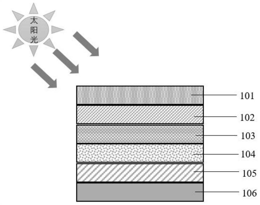
[0038] In this example, an organic-inorganic hybrid perovskite material was prepared and a perovskite solar cell was prepared using the material. The transparent substrate of the perovskite solar cell is quartz glass; the first transparent electrode layer is ITO with a thickness of 180nm; the hole transport layer is Spiro-OMeTAD with a thickness of 40nm; formed; the main component of the perovskite layer is Cs 0.05 (MA 0.13 FA 0.87 ) 0.95 Pb(I 0.87 Br 0.13 ) 3 , the thickness is 580nm; the electron transport layer is SnO 2 , with a thickness of 30nm; the second electrode layer is gold with a thickness of 80nm. The preparation steps of perovskite solar cells are as follows:
[0039] (1) ITO conductive glass is cleaned with glass cleaning solution, acetone, and ethanol in sequence, and after drying, use an ultraviolet ozone cleaner to remove residual organic matter.
[0040] (2) 360μL SnO 2 Mixed with 2.4mL deionized water, prepared SnO by spin coating method 2 After ...
Embodiment 2
[0045] In this example, an organic-inorganic hybrid perovskite material was prepared and a perovskite solar cell was prepared using the material. The transparent substrate of the perovskite solar cell is quartz glass; the first transparent electrode layer is ITO with a thickness of 180nm; the electron transport layer is SnO 2 , with a thickness of 30nm; the perovskite layer is (FAPbI 3 ) 1-x-y (MAPbBr 3 ) x ) (MAPbCl 3 ) y ), where x, y, and 1-x-y are greater than or equal to 0 and less than or equal to 1 respectively, and the thickness is 700nm; the hole transport layer is Spiro-OMeTAD, and the thickness is 100nm; the second electrode layer is gold, and the thickness is 80nm. The preparation steps of the perovskite solar cell of the present embodiment are as follows:
[0046] (1) ITO conductive glass is cleaned with glass cleaning solution, acetone, and ethanol in sequence, and after drying, use an ultraviolet ozone cleaner to remove residual organic matter.
[0047] (...
PUM
| Property | Measurement | Unit |
|---|---|---|
| concentration | aaaaa | aaaaa |
| thickness | aaaaa | aaaaa |
| thickness | aaaaa | aaaaa |
Abstract
Description
Claims
Application Information


