SOI structure and manufacturing method thereof, MEMS device and manufacturing method thereof

A manufacturing method and device technology, which is applied in the field of SOI structure and manufacturing, and MEMS devices, can solve the problems that the reliability of devices cannot be effectively improved, and the insulation of isolation grooves is poor.

Active Publication Date: 2021-10-01
SEMICON MFG ELECTRONICS (SHAOXING) CORP
View PDF4 Cites 0 Cited by
  • Summary
  • Abstract
  • Description
  • Claims
  • Application Information

AI Technical Summary

Problems solved by technology

If the patent figure 1 The insulating layer structure shown is used to solve the problem of poor insulation of the isolation trench of MEMS devices, but it still cannot avoid the problem of lateral corrosion of the oxide layer at the bottom of both sides of the isolation trench during the etching process, and the reliability of the device cannot be effectively improved.

Method used


Image

  • SOI structure and manufacturing method thereof, MEMS device and manufacturing method thereof
  • SOI structure and manufacturing method thereof, MEMS device and manufacturing method thereof
  • SOI structure and manufacturing method thereof, MEMS device and manufacturing method thereof

Examples


Embodiment Construction

[0044] The following will clearly and completely describe the technical solutions in the embodiments of the present invention with reference to the drawings in the embodiments of the present invention.

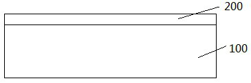
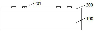
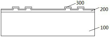
[0045] The following examples of this embodiment are all carried out by using the SOI structure as an example to realize isolation and insulation applications. First, an SOI structure and a method for manufacturing the SOI structure are disclosed, wherein the SOI structure is as follows Figure 6 As shown, it includes at least a first silicon layer 100 , an insulating layer and a second silicon layer 500 from bottom to top. The SOI structure (silicon on insulator) is often used in the manufacture of MEMS devices, and the buried oxide layer in the middle is mainly used to realize the insulation isolation between electrodes. Unlike the existing SOI structure that uses a silicon dioxide single-layer structure to form the buried oxide layer, the insulating layer in this embodiment...


PUM

PropertyMeasurementUnit
Thicknessaaaaaaaaaa
Thicknessaaaaaaaaaa
Deposition thicknessaaaaaaaaaa

Abstract

The invention relates to an SOI structure and a manufacturing method, and also relates to an MEMSdevice manufactured by utilizing the SOI structure and a method for manufacturing the MEMS device. An insulating layer of the SOI structure is mainly designed to be of a silicon oxide-silicon nitride-silicon oxide multilayer structure, a protruding retaining wall structure is formed on a silicon nitride layer, when an MEMS device is manufactured, an upper silicon dioxide layer is used as a stop layer for deep silicon etching of an isolation groove, it is guaranteed that deep silicon etching has enough process windows, and the fatal problem of short circuit caused by insufficient etching of the isolation groove is avoided; and when a mask layer for etching a comb tooth electrode and an isolation groove is removed, a VHF gas phase etching technology in an existing technology is replaced by a wet etching technology, a silicon nitride layer is used as a stop layer of wet etching, silicon nitride retaining wall structures on the two sides of the bottom of the isolation groove can effectively prevent lateral corrosion to the insulating layer in the wet etching process, and the insulating effect of the isolation groove and the reliability of the device can be improved.

Description

technical field [0001] The invention relates to the technical field of semiconductor manufacturing, in particular to an SOI structure and a manufacturing method, and also to a MEMS device made with the SOI structure and a method for manufacturing the MEMS device. Background technique [0002] SOI (Silicon-On-Insulator) is silicon on insulating layer. This technology is a multi-layer structure formed by introducing a buried oxide layer between the top silicon and the back substrate silicon. Due to the unique advantages of the SOI structure, devices based on this structure will substantially reduce junction capacitance and leakage current, increase switching speed, reduce power consumption, and achieve high-speed, low-power operation. Its performance is significantly better than bulk silicon devices and circuit. At present, devices manufactured with SOI structures have been widely used in most fields of microelectronics, and are also applied in other fields such as optoelectr...

Claims


Application Information

Patent Timeline
IPC IPC(8): H01L27/12H01L21/762B81B7/02B81C1/00
CPCH01L27/1203H01L21/76251B81B7/02B81C1/00555B81C1/00571
Inventor 蔡双
Owner SEMICON MFG ELECTRONICS (SHAOXING) CORP
Why Eureka
Try Eureka