CIS board-level fan-out packaging structure based on plastic through holes and manufacturing method thereof

A technology of packaging structure and manufacturing method, which is applied in the directions of radiation control devices, semiconductor/solid-state device manufacturing, electrical components, etc., can solve problems such as difficult to deal with the application of products with high integration, long relative process flow, and complicated process flow, etc. Achieve the effect of simplifying the installation alignment process, simplifying the difficulty of production, and simplifying the circuit structure

Pending Publication Date: 2021-10-08
JIHUA LAB
View PDF5 Cites 0 Cited by
  • Summary
  • Abstract
  • Description
  • Claims
  • Application Information

AI Technical Summary

Problems solved by technology

Among them, the COB module packaging method generally uses copper clad boards such as PCB or FPC for chip fixing, bonding wire interconnection, and prism system installation.
Another CIS module packaging technology is CSP packaging. The TSV fan-out packaging technology currently used in this package has a relatively long process flow.

Method used


Image

  • CIS board-level fan-out packaging structure based on plastic through holes and manufacturing method thereof
  • CIS board-level fan-out packaging structure based on plastic through holes and manufacturing method thereof
  • CIS board-level fan-out packaging structure based on plastic through holes and manufacturing method thereof

Examples


Embodiment Construction

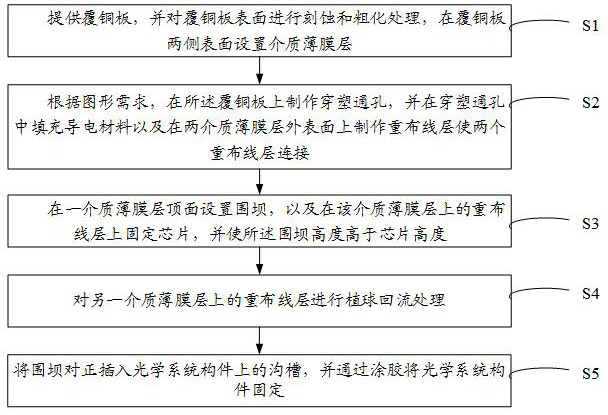
[0041] Embodiments of the present invention are described in detail below, examples of which are shown in the drawings, wherein the same or similar reference numerals designate the same or similar elements or elements having the same or similar functions throughout. The embodiments described below by referring to the figures are exemplary only for explaining the present invention and should not be construed as limiting the present invention.

[0042] In describing the present invention, it should be understood that the terms "center", "longitudinal", "transverse", "length", "width", "thickness", "upper", "lower", "front", " Orientation indicated by rear, left, right, vertical, horizontal, top, bottom, inside, outside, clockwise, counterclockwise, etc. The positional relationship is based on the orientation or positional relationship shown in the drawings, which is only for the convenience of describing the present invention and simplifying the description, rather than indicati...


PUM


Abstract

The invention discloses a CIS board-level fan-out packaging structure based on plastic through holes and a manufacturing method thereof. The manufacturing method comprises the following steps of providing a copper-clad plate, carrying out the etching and roughening of the surface of the copper-clad plate, and arranging dielectric film layers on the surfaces of the two sides of the copper-clad plate, manufacturing a plastic through hole in the copper-clad plate, filling a conductive material in the plastic through hole, and manufacturing a rewiring layer on the outer surfaces of the two dielectric film layers, arranging a box dam on the top surface of a dielectric film layer, and fixing a chip on the rewiring layer on the dielectric film layer, carrying out reballing reflow treatment on the rewiring layer on the other dielectric film layer, and aligning and inserting the box dam into the groove on the optical system component, and fixing the optical system component through gluing. According to the manufacturing method, the production difficulty and process are effectively simplified, and the manufacturing efficiency of the packaging body is effectively improved; secondly, the box dam is arranged to replace an existing base support to be in butt joint with the optical system component, and the installation and alignment process of the optical system component is simplified.

Description

technical field [0001] The invention belongs to the technical field of semiconductors, and in particular relates to a CIS board-level fan-out packaging structure based on through-plastic through holes and a manufacturing method thereof. Background technique [0002] With the upgrading of consumer electronics, the application of the Internet of Things and the development of the Internet of Vehicles, the transmission speed, heat dissipation and miniaturization of high-definition and high-speed camera chips pose new technical challenges. [0003] CIS (Contact Image Sensor) is a photoelectric conversion device that uses a column of built-in LED light-emitting diodes to directly contact and read image data on the surface of the original. CIS generally includes a chip part with a circuit structure and I / O ports and an optical system component connected through a base bracket. The optical system component generally includes a Len lens, a VCM voice coil motor, and the like. [0004...

Claims


Application Information

Patent Timeline
Patent Type & Authority Applications(China)
IPC IPC(8): H01L27/146H01L21/78
CPCH01L27/14618H01L27/14636H01L27/1469H01L27/14683
Inventor 李潮杨斌贺姝敏成海涛崔成强林挺宇
Owner JIHUA LAB
Why Eureka
Try Eureka