Semiconductor packaging structure and preparation method thereof

A packaging structure and semiconductor technology, applied in semiconductor/solid-state device manufacturing, semiconductor devices, semiconductor/solid-state device components, etc., can solve the problems of difficulty in ensuring vertical interconnection of different layers, low integration of antenna packaging structures, and high packaging costs , to achieve the effect of saving production and development costs, meeting the requirements of three-dimensional packaging, good electrical and thermal performance and high-efficiency antenna performance

Pending Publication Date: 2021-10-12
SJ SEMICON JIANGYIN CORP
View PDF0 Cites 4 Cited by
  • Summary
  • Abstract
  • Description
  • Claims
  • Application Information

AI Technical Summary

Problems solved by technology

[0005] In view of the above-mentioned shortcomings of the prior art, the purpose of the present invention is to provide a semiconductor packaging structure and its preparation method, which are used to solve the problems of low integration of the antenna packaging structure, high packaging cost, and difficulty in ensuring different layers in the prior art. Vertical interconnection, and the low efficiency of the antenna, etc.

Method used


Image

  • Semiconductor packaging structure and preparation method thereof
  • Semiconductor packaging structure and preparation method thereof
  • Semiconductor packaging structure and preparation method thereof

Examples


Embodiment 1

[0052] Such as figure 1 As shown, the present invention provides a kind of preparation method of semiconductor package structure, and described preparation method comprises steps:

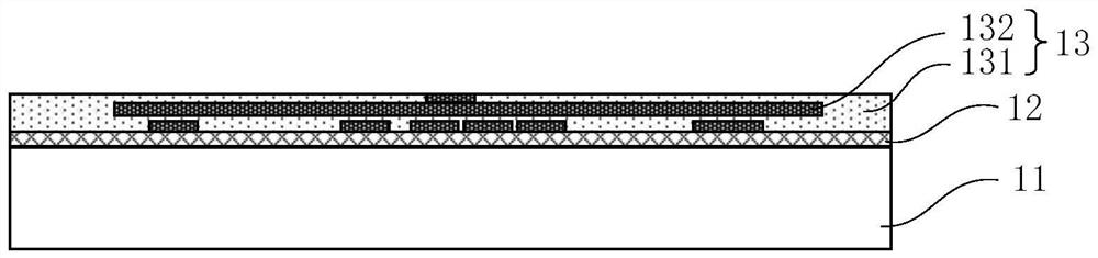
[0053] S1: providing a substrate 11, forming a light-to-heat conversion material layer 12 on the upper surface of the substrate 11;

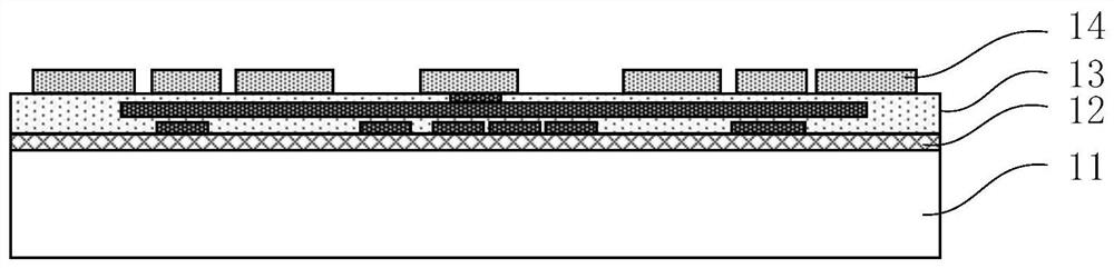
[0054] S2: Form a rewiring layer 13 on the upper surface of the light-to-heat conversion material layer 12, the rewiring layer 13 includes a dielectric layer 131 and a metal connection layer 132 located in the dielectric layer 131, specifically as figure 2 shown;

[0055] S3: Form the first antenna layer 14 on the upper surface of the rewiring layer 13, the first antenna layer 14 is electrically connected to the rewiring layer 13 (more precisely, it is electrically connected to the metal connection layer 132 ), specifically as image 3 shown;

[0056] S4: Form a conductive column 15 on the upper surface of the first antenna layer 14 through an electroplating pro...

Embodiment 2

[0079] Such as Figure 12As shown, the present invention also provides a semiconductor packaging structure, which can be prepared based on the preparation method of the first embodiment, so the description of the relevant structural layers in the first embodiment is fully applicable to this embodiment. Specifically, the semiconductor package structure includes a substrate 11, a light-to-heat conversion material layer 12, a rewiring layer 13, a first antenna layer 14, a conductive column 15, a plastic packaging material layer 16, a second antenna layer 17, a metal bump 18 and chip 19; the light-to-heat conversion material layer 12 is located on the upper surface of the substrate 11; the rewiring layer 13 is located on the upper surface of the light-to-heat conversion material layer 12, and the rewiring layer 13 includes a dielectric layer 131 and The metal connection layer 132 located in the dielectric layer 131; the first antenna layer 14 is located on the upper surface of the...


PUM

PropertyMeasurementUnit
thicknessaaaaaaaaaa

Abstract

The invention provides a semiconductor packaging structure and a preparation method thereof. The structure comprises a substrate, a photothermal conversion material layer, a rewiring layer, a first antenna layer, a conductive column, a plastic package material layer, a second antenna layer, a metal bump and a chip, the photothermal conversion material layer is located on the upper surface of the substrate; the rewiring layer is located on the upper surface of the photothermal conversion material layer; the first antenna layer is located on the upper surface of the rewiring layer; the conductive columns are located on the upper surface of the first antenna layer; the plastic package material layer wraps the first antenna layer and the conductive column, and the upper surface of the conductive column is exposed on the upper surface of the plastic package material layer; the second antenna layer is located on the upper surface of the plastic package material layer; the metal bump is located on the upper surface of the second antenna layer; and the chip is located on the upper surface of the metal bump. According to the invention, interconnection of the chip and the plurality of antenna layers in the vertical direction can be realized to ensure good conduction of the upper layer and the lower layer, the size of the packaging structure can be reduced, the integration level and the performance of the device can be improved, and the production cost can be reduced.

Description

technical field [0001] The invention belongs to the field of semiconductor packaging, in particular to a semiconductor packaging structure and a preparation method thereof. Background technique [0002] With the advent of the 5G era, in order to meet the high-capacity communication needs, new spectrums are continuously introduced, which makes the requirements for antennas higher and higher. In order to ensure the quality of signal reception, portable mobile terminals such as mobile phones usually have built-in antenna structures for communication functions, such as realizing voice and video connections and surfing the Internet. At present, the common method of building the antenna is to directly fabricate the antenna on the surface of the circuit board. However, due to the additional area of ​​the circuit board occupied by the antenna, the integration of the device is poor, which restricts the further miniaturization of the mobile communication terminal. At the same time, d...

Claims


Application Information

Patent Timeline
Patent Type & Authority Applications(China)
IPC IPC(8): H01L23/66H01L23/498H01L21/48H01L21/60H01L23/34H01Q1/22
CPCH01L23/66H01L23/49827H01L23/49822H01L24/81H01L21/4857H01L21/486H01L23/345H01Q1/2283H01L2223/6677
Inventor 黄晗林正忠吴政达陈彦亨
Owner SJ SEMICON JIANGYIN CORP
Why Eureka
Try Eureka