Semiconductor wafer cutting device

A cutting device and semiconductor technology, which is applied to fine working devices, cleaning methods using gas flow, working accessories, etc., can solve the problems of diamond graphitization, affecting the service life of the cutting disc, and the cutting disc being easily burnt and falling off. To achieve the effect of ensuring cleanliness and improving service life

Inactive Publication Date: 2021-10-19
高彬
View PDF0 Cites 5 Cited by
  • Summary
  • Abstract
  • Description
  • Claims
  • Application Information

AI Technical Summary

Problems solved by technology

[0004] The purpose of the present invention is to solve the problem that the semiconductor wafer acquisition method in the prior art is to cut the raw material silicon to obtain the target wafer, and in order to improve the flatness of the wafer surface obtained after cutting, diamond cutting sheets are usually used for cutting work, but During the cutting process, a large amount of heat is generated on the surface of the cutting piece, and the heat is easy to graphitize the diamond, and the cutting disk is also easily burned and peeled off, thereby affecting the service life of the cutting piece, and a semiconductor wafer cutting device is proposed

Method used


Image

  • Semiconductor wafer cutting device
  • Semiconductor wafer cutting device
  • Semiconductor wafer cutting device

Examples


Embodiment 1

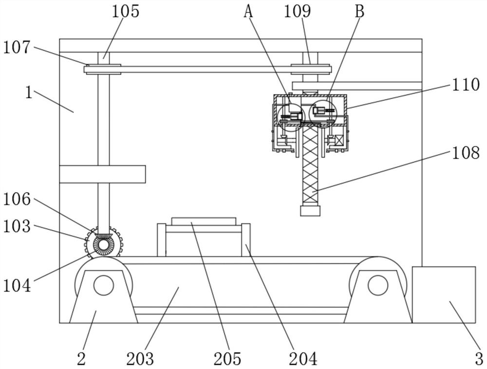
[0032] refer to Figure 1-7, a semiconductor wafer cutting device, comprising a vertical plate 1, a fixed plate 2 and a silicon body 205, the vertical plate 1 is fixedly connected with a first motor 102, the output shaft of the first motor 102 is connected with a first bevel gear 104, the vertical The plate 1 is rotatably connected with a first rotating shaft 105, the bottom of the first rotating shaft 105 is fixedly connected with a second bevel gear 106 meshing with the first bevel gear 104, and the side wall of the riser 1 is rotatably connected with a reciprocating screw rod 108. A rotating shaft 105 and the reciprocating screw mandrel 108 are connected by a first belt, the reciprocating screw mandrel 108 is threadedly connected with a slide box 110, the bottom of the slide box 110 is provided with a cutting mechanism, and the bottom of the slide box 110 is provided with a drive cutting mechanism. The second motor 111 is equipped with a cooling mechanism and a cleaning mec...

Embodiment 2

[0037] refer to figure 1 , Figure 4 with Figure 5 , is basically the same as Embodiment 1, furthermore, in order to cut the silicon body, the cutting mechanism includes a first cutting disc 113 and a second cutting disc 119, and the output end of the second motor 111 is fixedly connected with a second rotating shaft 112, The first cutting disc 113 is fixedly connected to the second rotating shaft 112, the third rotating shaft 114 and the fourth rotating shaft 116 are respectively connected to rotate in the slide box 110, and a bevel gear set 1 is connected between the third rotating shaft 114 and the second rotating shaft 112, The third pulley 115 is fixedly connected on the third rotating shaft 114, the fourth pulley 117 is fixedly connected on the fourth rotating shaft 116, the second belt is connected between the third pulley 115 and the fourth pulley 117, and the slide box 110 The bottom of the bottom is rotatably connected with a fifth rotating shaft 118, the second c...

Embodiment 3

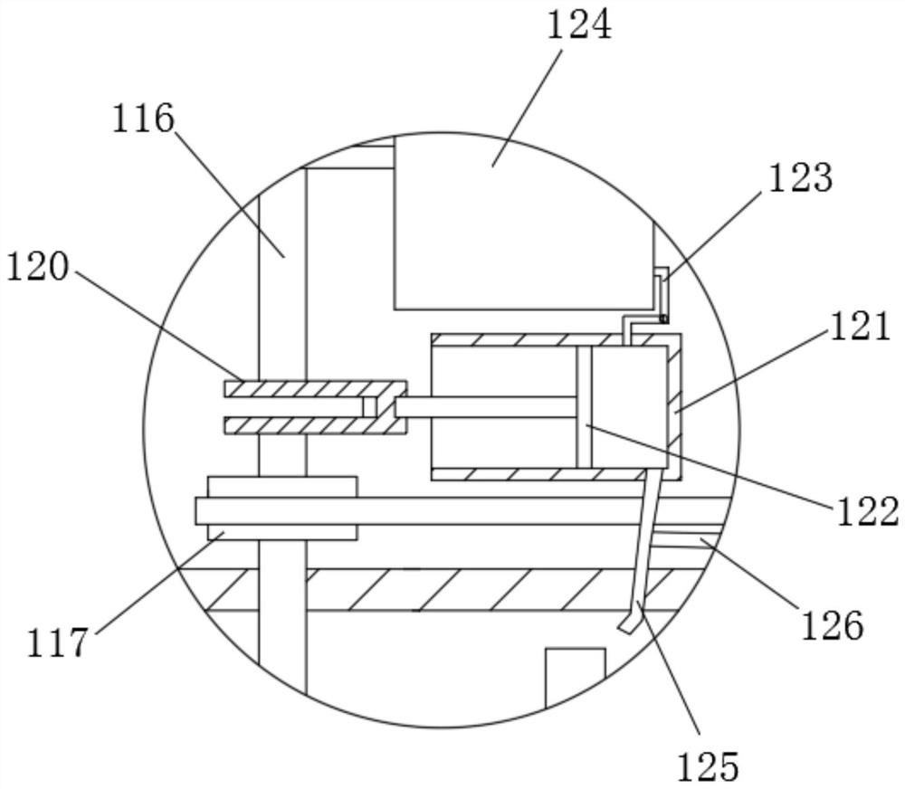
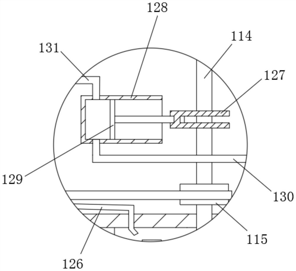
[0043] refer to figure 1 , figure 2 with Figure 5 , is basically the same as Embodiment 1, furthermore, in order to lower the temperature of the cutting mechanism, the cooling mechanism includes a coolant tank 124, a first crankshaft 120, a first connection box 121 and a first piston 122, a coolant tank 124 and a first piston 122 A connecting box 121 is fixedly connected in the slide box 110, the first piston 122 is slidably connected in the first connecting box 121, the first crankshaft 120 is fixedly connected on the fourth rotating shaft 116, and the outer wall of the first crankshaft 120 is rotatably connected with a second A connecting rod, the end of the first connecting rod away from the first crankshaft 120 is connected to the side wall of the first piston 122 in rotation, and a liquid suction pipe 123 is connected between the first connection box 121 and the coolant tank 124, and the liquid suction pipe 123 A one-way valve is provided, the side wall of the first c...


PUM


Abstract

The invention discloses a semiconductor wafer cutting device, and belongs to the technical field of semiconductors. The semiconductor wafer cutting device comprises a vertical plate, a fixing plate and a silicon body, wherein the vertical plate is fixedly connected with a first motor; an output shaft of the first motor is connected with a first bevel gear; the vertical plate is rotationally connected with a first rotating shaft; the bottom of the first rotating shaft is fixedly connected with a second bevel gear in meshed connection with the first bevel gear; the side wall of the vertical plate is rotationally connected with a reciprocating screw rod; the first rotating shaft is connected with the reciprocating screw rod through a first belt; the reciprocating screw rod is in threaded connection with a sliding box; a cutting mechanism is arranged at the bottom of the sliding box; and a second motor for driving the cutting mechanism is arranged at the bottom of the sliding box. According to the semiconductor wafer cutting device, a cutting disc can be rapidly cooled, the service life of the cutting disc is prolonged, chippings generated after cutting can be cleaned, the surface of a wafer is guaranteed to be clean, and follow-up machining is facilitated.

Description

technical field [0001] The invention relates to the technical field of semiconductors, in particular to a semiconductor wafer cutting device. Background technique [0002] Semiconductors refer to materials whose conductivity is between conductors and insulators at room temperature. Semiconductors are used in integrated circuits, consumer electronics, communication systems, photovoltaic power generation, lighting, high-power power conversion and other fields. For example, diodes are devices made of semiconductors. , no matter from the perspective of technology or economic development, the importance of semiconductors is huge. The core units of most electronic products, such as computers, mobile phones or digital recorders, are closely related to semiconductors. Common semiconductor materials include silicon, germanium, gallium arsenide, etc. Silicon is one of the most important semiconductor materials in the application One of the most influential. In chip manufacturing, a ...

Claims


Application Information

Patent Timeline
Patent Type & Authority Applications(China)
IPC IPC(8): B28D5/02B28D7/00B28D7/04B28D7/02B08B5/02B08B13/00
CPCB28D5/029B28D5/023B28D5/0058B28D5/0082B28D5/0076B08B5/02B08B13/00
Inventor 不公告发明人
Owner 高彬
Why Eureka
Try Eureka