Preparation method of bipolar gating memristor and bipolar gating memristor

A memristor and gating technology, applied in the direction of electrical components, etc., can solve the problems such as the difficulty and complexity of process preparation, and achieve the effect of increasing the number of pulse erasing and writing, reducing the difference, and improving the holding capacity

Active Publication Date: 2021-10-19
HUAZHONG UNIV OF SCI & TECH
View PDF8 Cites 0 Cited by
  • Summary
  • Abstract
  • Description
  • Claims
  • Application Information

AI Technical Summary

Problems solved by technology

[0005] Aiming at the defects of the prior art, the object of the present invention is to provide a method for preparing a bipolar gating memristor and a bipolar gating memristor, aiming at solving the problem of the existing high-performance bipolar gating device preparation process The difficulty is more complicated, such as the need to pr

Method used


Image

  • Preparation method of bipolar gating memristor and bipolar gating memristor
  • Preparation method of bipolar gating memristor and bipolar gating memristor
  • Preparation method of bipolar gating memristor and bipolar gating memristor

Examples


preparation example Construction

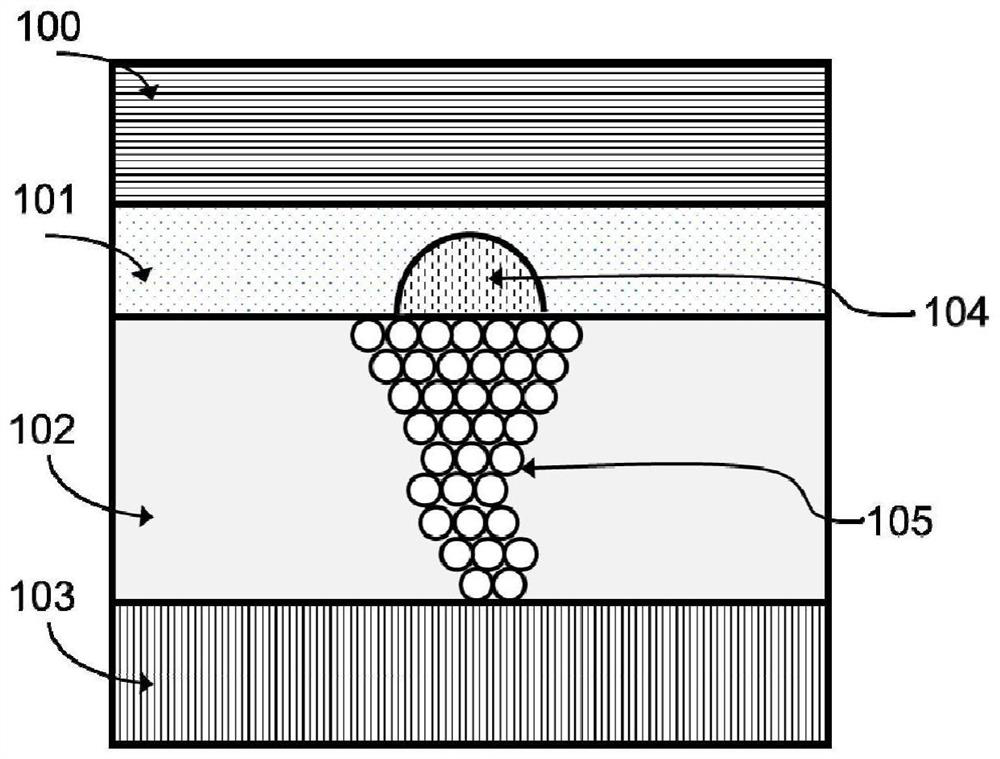
[0034] To this end, the present invention proposes a new type of memristive device structure with built-in bipolar gating and its preparation method. The device based on this reliable structure shows excellent overall performance improvement, such as free of large voltage initialization process, preparation at room temperature , simple structure, excellent performance in various operating modes, and no high-temperature annealing step. The cross-array stacking structure of the built-in bipolar gating memristor based on the present invention will provide a hardware foundation for the next generation of non-volatile storage, full memristive neural network architecture, and reconfigurable logic circuits.

[0035] The present invention aims at the above-mentioned existing process preparation problems, and provides a gating memristor and its preparation method, which form excellent built-in bipolar gating characteristics through the spontaneous oxidation process of the upper electrod...


PUM

PropertyMeasurementUnit
Thicknessaaaaaaaaaa
Thicknessaaaaaaaaaa
Thicknessaaaaaaaaaa

Abstract

The invention provides a preparation method of a bipolar gating memristor and a bipolar gating memristor. The preparation method comprises the following steps of: preparing a lower electrode; depositing a resistive material layer on the lower electrode; and depositing an upper electrode on the resistive material layer, specifically, depositing the upper electrode by adopting a magnetron sputtering mode, controlling sputtering power to control metal particles of the upper electrode to have proper kinetic energy, and controlling the vacuum degree of an area where the upper electrode and the resistive material layer are located, so as to enable the upper electrode and the resistive material layer to spontaneously generate oxidation-reduction reaction in the deposition process of the upper electrode so as to form a built-in bipolar gating layer, and further depositing the upper electrode on the built-in bipolar gating layer, or selecting a material with the activity higher than that of metal elements of the resistive material layer as a metal material of the upper electrode, so as to make the upper electrode and the resistive material layer spontaneously generate oxidation-reduction reaction in the deposition process of the upper electrode, so as to form a built-in bipolar gating layer and further depositing the upper electrode on the built-in bipolar gating layer. According to the preparation method of the bipolar gating memristor and the bipolar gating memristor of the invention, the performance of the bipolar gating device is improved.

Description

technical field [0001] The invention belongs to the field of microelectronic devices, and more specifically relates to a preparation method of a bipolar gating memristor and a bipolar gating memristor. Background technique [0002] In the context of the Internet of Things era, unprecedented data volume growth is driving the development of high-efficiency, cheap, and micro-storage technologies. Due to the bottleneck of Moore's Law, the continued scaling of Complementary Metal Oxide Semiconductor (CMOS) will bring about a substantial increase in cost. In recent years, memristors, which are cheap, simple in structure, scalable, low in power consumption, reliable, and nonvolatile, have become one of the most promising storage technologies for logistics network applications. Due to the simple sandwich device structure, memristors are suitable for large-scale 2D or 3D integration using passive cross-array structures. The characteristic of the interleaved array structure is that ...

Claims


Application Information

Patent Timeline
IPC IPC(8): H01L45/00
CPCH10N70/821H10N70/026H10N70/826H10B63/22H10B63/84H10N70/245
Inventor 李祎何毓辉付瑶瑶黄晓弟缪向水
Owner HUAZHONG UNIV OF SCI & TECH
Why Eureka
Try Eureka