Micro light emitting diode and manufacturing method thereof

A technology of a micro light-emitting diode and a manufacturing method, which is applied to electrical components, circuits, semiconductor devices, etc., can solve the problems of low full-colorization efficiency, difficult circuit design of display panels, and low color conversion efficiency of green light quantum dots, etc. Efficiency, the effect of improving color conversion efficiency

Pending Publication Date: 2021-10-22
CHONGQING KONKA PHOTOELECTRIC TECH RES INST CO LTD
View PDF0 Cites 0 Cited by
  • Summary
  • Abstract
  • Description
  • Claims
  • Application Information

AI Technical Summary

Problems solved by technology

[0003] At present, there are two methods for micro-LED chips to be used in full-color AR micro-displays and mobile/large-scale displays. One is to use three primary colors (Red Green Blue, RGB) micro-LEDs for natural color mixing; the other is to use quantum dots (Quantum Dots, QDs) + blue micro-LED chip, if using RGB micro-LED chips,

Method used


Image

  • Micro light emitting diode and manufacturing method thereof
  • Micro light emitting diode and manufacturing method thereof
  • Micro light emitting diode and manufacturing method thereof

Examples


Embodiment 1

[0041] like figure 1 Shown is a micro light emitting diode according to the present invention.

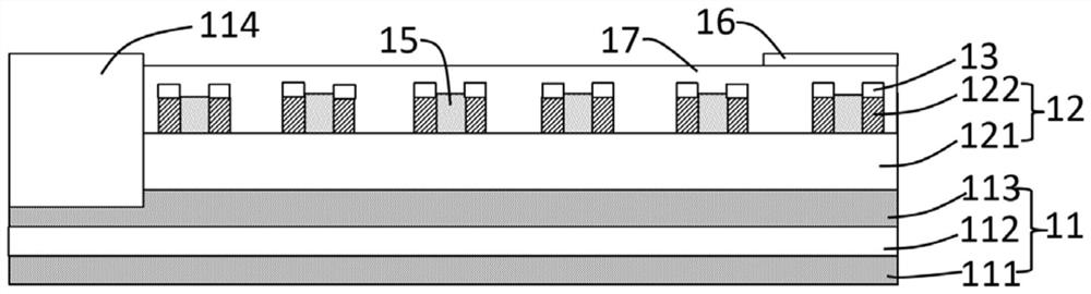
[0042] The specific structure is as figure 1 As shown, it includes a first semiconductor layer 11 , an active layer 12 and a second semiconductor layer 13 .

[0043] The first semiconductor layer 11 is an N-type semiconductor, more preferably GaN, which is a new generation of energy material and is widely used in light emitting diodes.

[0044] The first semiconductor layer 11 includes a low-temperature GaN layer 111 , and an undoped GaN layer 112 , an N-type GaN layer 113 , and an N-type GaN layer 113 are sequentially stacked on the low-temperature GaN layer 11 .

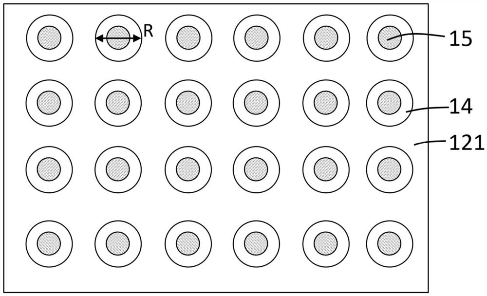
[0045] The active layer 12 is a quantum well layer, and the active layer 12 is composed of multiple pairs of quantum wells. The active layer 12 includes a first quantum well layer 121 and a second quantum well layer 122 . The quantum well layer in this embodiment is a green light quantum well layer, that is, it emit...

Embodiment 2

[0057] This embodiment is another light emitting diode structure of the micro light emitting diode.

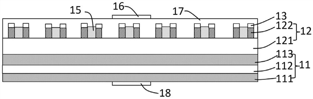
[0058] The specific structure is as image 3 As shown, it includes a first semiconductor layer 11 , an active layer 12 and a second semiconductor layer 13 .

[0059] The first semiconductor layer 11 is an N-type semiconductor, more preferably GaN, which is a new generation of energy material and is widely used in light emitting diodes.

[0060] The first semiconductor layer 11 includes a low-temperature GaN layer 111 , and an undoped GaN layer 112 , an N-type GaN layer 113 , and an N-type GaN layer 113 are sequentially stacked on the low-temperature GaN layer 11 .

[0061] The active layer 12 is a quantum well layer, and the active layer 12 is composed of multiple pairs of quantum wells. The active layer 12 includes a first quantum well layer 121 and a second quantum well layer 122 . The quantum well layer in this embodiment is a green light quantum well layer, that is, it ...

Embodiment 3

[0072] Such as Figure 4 Shown is the micro light emitting diode manufacturing method described in this application. Specific steps are as follows:

[0073] S10 provides a substrate 10 on which the first semiconductor layer 11 is formed.

[0074] Such as Figure 5 As shown, the first semiconductor layer 11 includes a low-temperature GaN layer 111 , an undoped GaN layer 112 and an N-type GaN layer 113 stacked once, and the substrate 10 is a sapphire substrate.

[0075] S11 forms the active layer 12 and the second semiconductor layer 13 on the first semiconductor layer 11 .

[0076] Such as Figure 6 As shown, the active layer 12 is a quantum well layer, which is composed of a first quantum well layer 121 and a second quantum well layer 122, and the second semiconductor layer 13 is formed on the second quantum well layer. The first semiconductor layer 11 and the second semiconductor layer 13 are different types of semiconductors. In this embodiment, the first semiconductor ...


PUM


Abstract

The invention relates to the field of light emitting diodes, and the light emitting diode comprises a first semiconductor layer, an active layer and a second semiconductor layer which are stacked in sequence, wherein the first semiconductor layer and the second semiconductor layer are different types of semiconductor layers, and the active layer comprises a first quantum well layer and a second quantum well layer which are stacked in sequence. A nanoring structure is formed on the second quantum well layer and the second semiconductor layer, the first quantum well layer emits light of a first color, the part, corresponding to the side wall of the nanoring, of the second quantum well layer emits light of a second color, the first color is different from the second color, the first semiconductor layer is electrically connected with a first electrode, and the second semiconductor layer is electrically connected with a second electrode. The invention further comprises a manufacturing method of the micro light-emitting diode, the nanometer silicon dioxide particles are used as a photomask to manufacture the nanometer ring, the original quantum well stress is released, the quantum limited stark effect is reduced, and blue light is generated.

Description

technical field [0001] The invention relates to the technical field of manufacturing LED display devices, in particular to a micro light emitting diode and a manufacturing method thereof. Background technique [0002] A general light-emitting diode (Light-Emitting Diode, LED) chip includes a substrate and an epitaxial layer, the thickness of which is about 100-500 μm, and the size is between 100-1000 μm. The further ongoing research on micro-LED display panels is to physically or chemically lift off the epitaxial layer with a thickness of about 4-5 μm on the surface of the LED, and then transplant it onto the circuit substrate. The micro-LED display integrates the two major technical characteristics of thin film transistor liquid crystal display (TFT-LCD) and LED. The development of materials, process and equipment is relatively mature, and the product specifications are much higher than the current TFT-LCD or organic light-emitting. Organic Light-Emitting Diode (OLED), whi...

Claims


Application Information

Patent Timeline
IPC IPC(8): H01L33/06H01L33/20H01L33/08H01L33/32H01L33/14H01L33/00
CPCH01L33/06H01L33/20H01L33/08H01L33/32H01L33/14H01L33/0075
Inventor 杨顺贵黄国栋林雅雯黄嘉宏
Owner CHONGQING KONKA PHOTOELECTRIC TECH RES INST CO LTD
Why Eureka
Try Eureka